
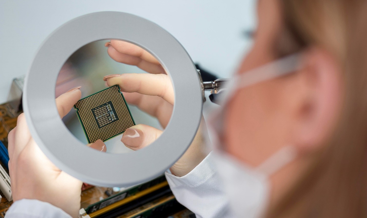
Introduction
For more than fifty years, progress in semiconductors followed one simple idea: make the transistor smaller, and everything gets faster, cheaper, and more efficient. This was the heart of Moore’s Law. But as chips approach the size of just a few atoms, simply shrinking transistors is no longer enough. The industry has had to get creative, and the result is a wave of genuinely new ideas, not just in the transistor itself, but in how chips are powered, printed, connected, and packaged.
The push is being driven hard by artificial intelligence. AI chips need to move huge amounts of data at very high speed while using as little power as possible, and that demand is reshaping the entire industry roadmap. Below are four of the most important innovations defining semiconductors in 2026, along with one bonus technology worth watching. Together they show how the center of gravity is shifting from pure transistor scaling toward smarter power delivery, advanced printing, and next-generation packaging.
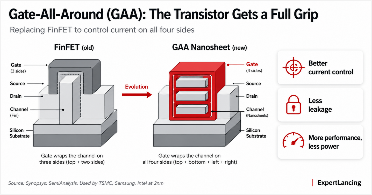
1. Gate-All-Around (GAA) Transistors
This is the most important structural change in transistor design in nearly a decade, replacing the FinFET architecture that dominated since around 2011. In a GAA transistor, often called a nanosheet transistor, the gate fully surrounds the channel on all four sides instead of just three, giving much better control over the flow of current and reducing leakage as transistors shrink. The practical payoff, according to design-tool maker Synopsys, is that GAA extends device scaling while increasing performance and cutting power consumption [Synopsys]. This is now the defining feature of the leading 2nm-class nodes that TSMC, Samsung, and Intel are ramping in the 2025-2026 window [SemiAnalysis].
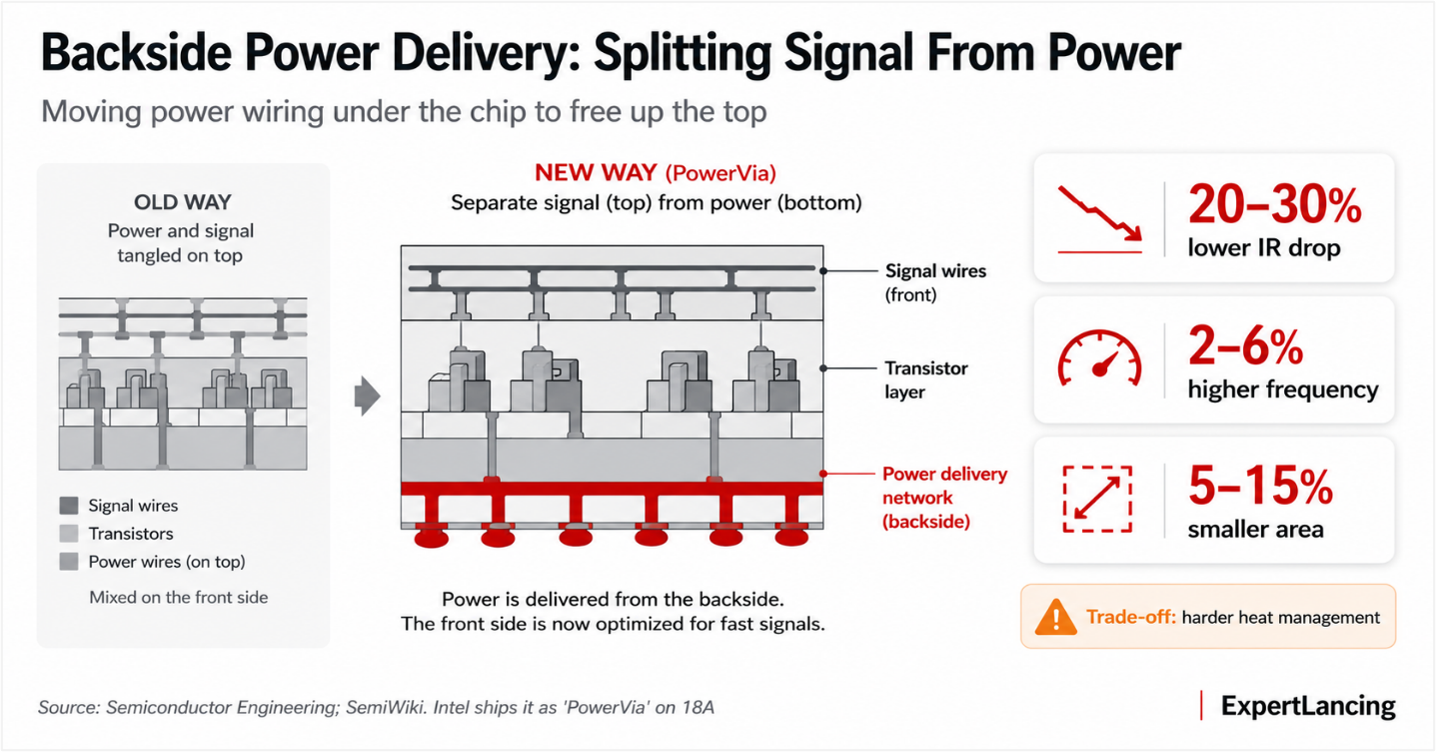
2. Backside Power Delivery (BSPDN / Intel’s PowerVia)
Traditionally, both the signal wires and the power wires sit on top of the transistors, where they compete for space and interfere with each other. Backside power delivery moves the power-delivery network to the underside of the wafer, freeing the front for signal routing and delivering cleaner power directly to the transistors. The measured benefits are substantial: industry analysis points to a 20-30% reduction in IR drop (voltage loss), a 2-6% increase in maximum operating frequency, and a 5-15% reduction in area [Semiconductor Engineering]. Intel commercialized its version, branded PowerVia, on its 18A process as a key part of its manufacturing comeback [SemiWiki]. The main challenge is thermal: with power on the back, heat dissipation becomes harder to manage.
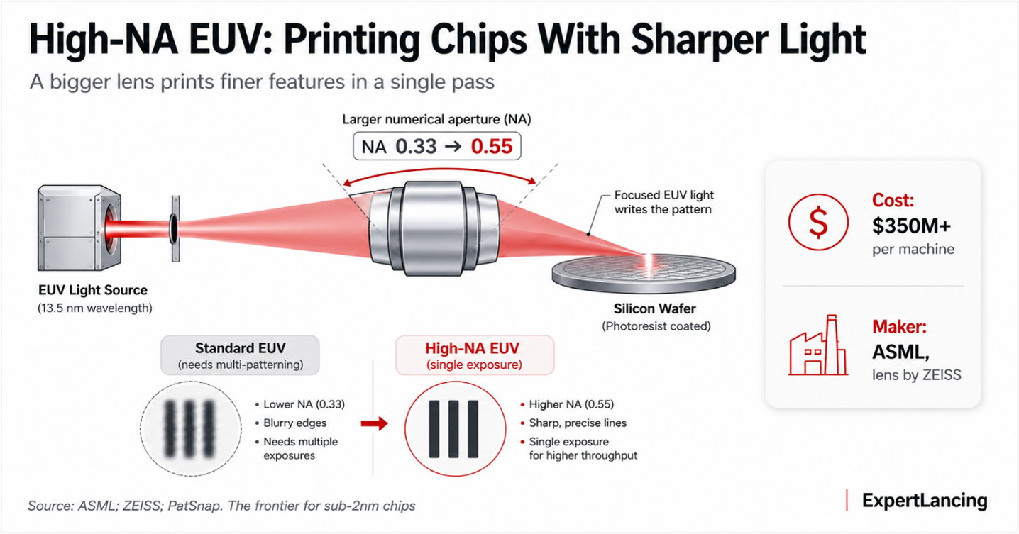
3. High-NA EUV Lithography
This is the next generation of the extreme-ultraviolet lithography used to print the finest features on chips. ASML‘s High-NA (high numerical aperture) machines increase the lens aperture from 0.33 to 0.55, which sharpens resolution and allows printing of much smaller features in a single exposure rather than relying on complex multi-patterning. ASML describes it as a major leap enabling the ultra-fine features required by the next generation of chips [ASML], and lens partner ZEISS frames it as the next technological leap for the industry [ZEISS]. It is widely viewed as the defining patterning frontier for sub-2nm semiconductors, though the tools are extraordinarily expensive and adoption is still in its early phase.
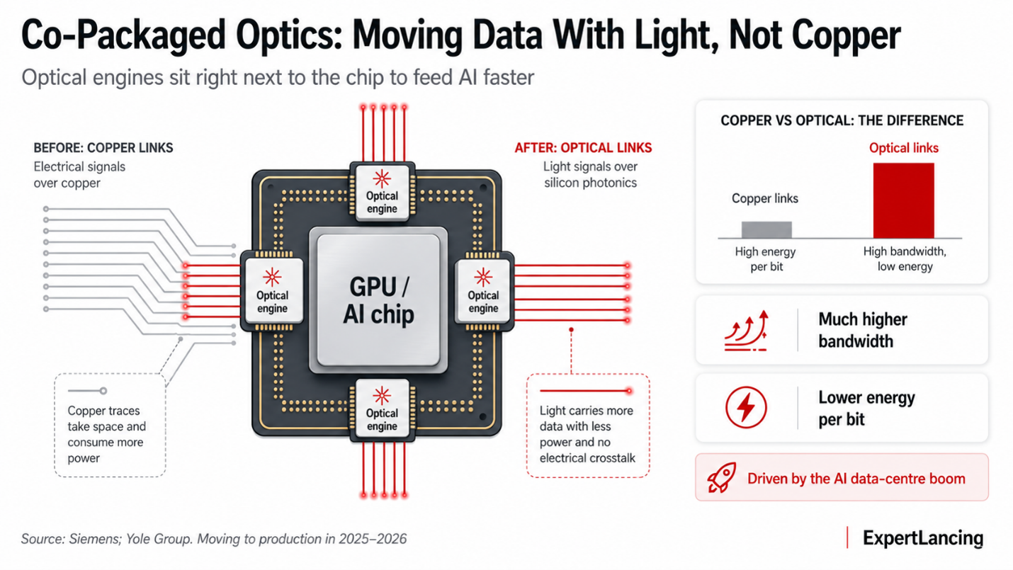
4. Co-Packaged Optics (CPO) and Silicon Photonics
Driven directly by the AI boom, this innovation tackles the data-movement bottleneck rather than the transistor itself. Instead of moving data between chips over copper wires, co-packaged optics integrates optical (light-based) engines right next to the processor or switch, dramatically increasing bandwidth while cutting energy per bit. Silicon photonics and optical interconnects are increasingly seen as the only viable path to sustain the bandwidth growth that AI data centers demand while controlling power consumption [Siemens]. Major players began moving CPO toward production for AI chips and network switches in the 2025-2026 period, according to research firm Yole Group [Yole Group].
Other Emerging Innovations to Watch
Beyond the four headline technologies, a few more innovations are reshaping the industry, mostly in packaging, materials, and memory rather than transistor shrinking.
Glass Core Substrates: The base layer that holds a chip is shifting from organic material to glass. Intel unveiled glass substrates that allow much higher interconnect density and better stability for large AI packages, with commercialization expected later this decade [Intel].
Chiplets and Hybrid Bonding: Instead of one big chip, designs are split into smaller chiplets and bonded copper-to-copper. AMD‘s 3D V-Cache uses hybrid bonding for roughly a 10x bandwidth gain, and SEMI calls it a cornerstone of 3D integration.
2D Materials and CFET: The likely next transistor frontier. CFET stacks transistors on top of each other, and atom-thin 2D materials keep performing where silicon is too thin. Research body imec sees these as the path to extend the roadmap, though they are still early-stage [imec].
Emerging Memory: New low-power, non-volatile memories like MRAM and FeRAM are gaining ground and being embedded directly into chips [IDTechEx].
Conclusion
These innovations tell a clear story about where the semiconductor industry is heading. The first two, gate-all-around transistors and backside power delivery, are about making the transistor itself better and more efficient. High-NA EUV lithography is about printing these tiny features with greater precision. And co-packaged optics, along with glass substrates, is about connecting and packaging chips so that data can move faster without wasting power.
The big takeaway is that the industry is no longer relying on transistor shrinking alone. The real action is moving toward packaging, power, and interconnect innovation, and artificial intelligence is the force pulling all of it forward. The companies that master not just how to build a smaller transistor, but how to power it, print it, and connect it efficiently, will lead the next phase of the chip race. In simple words, the future of semiconductors is no longer only about going smaller. It is about getting smarter at every layer of the chip.
At ExpertLancing, we turn patent, market, competitor, and technology signals into clear, research-backed decisions. If you are tracking disruptive shifts like these and want a defensible view before you make your next move, talk to our research team. Get in touch with ExpertLancing →