

At a glance
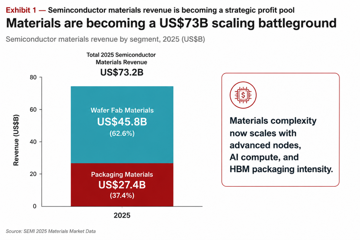
- Semiconductor materials are no longer background inputs. In 2025, the global semiconductor materials market reached a record US$73.2 billion, with wafer fab materials at US$45.8 billion and packaging materials at US$27.4 billion.
- AI, high-performance computing, and advanced memory are pulling materials innovation forward faster than traditional node roadmaps alone can explain. SIA reported April 2026 global semiconductor sales of US$110.5 billion, up sharply year on year, while citing WSTS expectations for a much larger 2026 market.
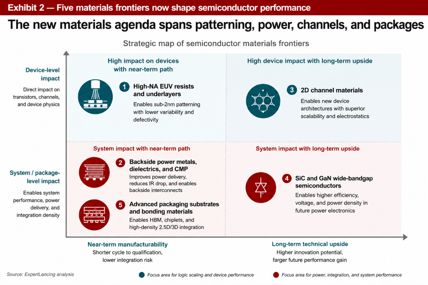
- The next performance gains will come from five material frontiers: High-NA EUV photoresists, backside power metals and dielectrics, 2D channel materials, wide-bandgap semiconductors, and advanced packaging substrates.
- The strategic shift is clear: materials suppliers are becoming co-architects of chip performance, yield, energy efficiency, and regulatory resilience.
Materials Have Moved from Consumables to Architecture
For decades, semiconductor strategy was narrated through lithography, transistor density, and fab capacity. Materials were important, but they were often treated as enabling consumables: silicon wafers, gases, chemicals, CMP slurries, targets, photoresists, substrates, encapsulants.
SEMI’s 2025 data show why. Wafer fab materials revenue rose to US$45.8 billion, while packaging materials reached US$27.4 billion [SEMI]. SEMI attributed the growth to higher process complexity, advanced-node demand, high-performance computing, and HBM-related packaging intensity. Lithography-related materials, including photomasks, photoresists, ancillaries, and wet chemicals, posted particularly strong growth.
The material stack is becoming a system-level design variable. A resist can determine whether High-NA EUV delivers usable yield. A dielectric can determine whether backside power reduces resistance without creating reliability problems. A substrate can determine whether chiplets communicate at acceptable bandwidth and thermal load. A silicon carbide crystal can determine whether an EV inverter becomes smaller, cooler, and more efficient.
The industry is not simply scaling transistors. It is scaling materials complexity.
High-NA EUV Turns Chemistry into A Bottleneck
High-NA EUV is often described as a lithography equipment transition. That is only half true. It is also a chemistry, mask, metrology, etch, and defect-control transition.
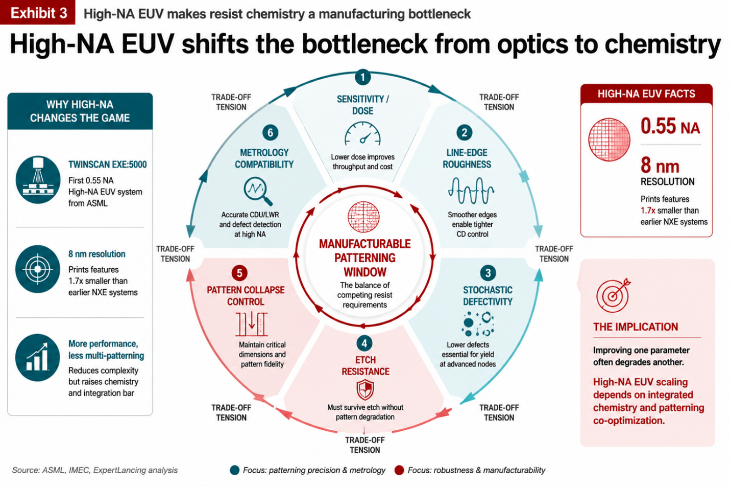
ASML’s first High-NA EUV platform, the TWINSCAN EXE:5000, uses a 0.55 numerical aperture [ASMI] and is designed to support 8 nm resolution [IMEC], enabling smaller features and potentially reducing multi-patterning complexity versus earlier EUV systems. But the tool alone does not create manufacturable chips. IMEC has emphasized that raising numerical aperture from 0.33 to 0.55 forces re-engineering across photoresist chemistry, etching, and metrology. In March 2026, IMEC received ASML’s EXE:5200 High-NA EUV system for sub-2 nm logic and high-density memory R&D, with full qualification expected by Q4 2026 [IMEC, IMEC].
This creates a difficult materials trade-off. EUV resists must deliver high sensitivity, low line-edge roughness, low stochastic defectivity, etch resistance, and pattern collapse control. Improving one parameter can worsen another. Chemically amplified resists, metal-oxide resists, underlayers, rinses, and developer chemistries are all being pulled into the same optimization loop.
The implication is strategic. Foundries and IDMs cannot evaluate lithography roadmaps separately from resist suppliers, mask shops, metrology vendors, and etch chemistry partners. The next node will be won by integrated patterning ecosystems, not by scanner procurement alone.
Backside Power Makes Metals, Dielectrics, and CMP Strategic
Backside power delivery is another example of materials becoming architecture. The logic is simple: move power delivery to the back side of the wafer, free up front-side routing resources, reduce resistance, and improve standard-cell utilization. The execution is not simple.
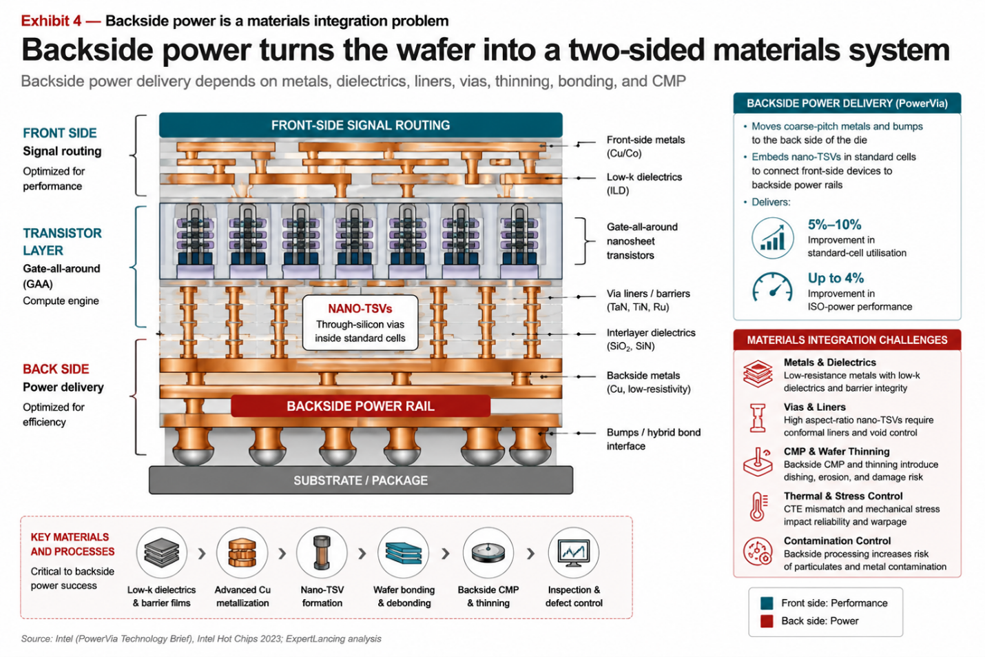
Intel’s 18A process combines RibbonFET gate-all-around transistors with PowerVia backside power delivery [Intel]. Intel says PowerVia relocates coarse-pitch metals and bumps to the back side of the die, embeds nanoscale through-silicon vias, and can improve standard-cell utilization by 5% to 10% while improving ISO-power performance by up to 4% [Intel]. TSMC has also positioned backside power as a major performance lever. Its A16 technology, expected to enter production in the second half of 2026 [semiengineering], combines nanosheet transistors with a backside power approach called Super Power Rail, targeted initially at demanding AI chips [TSMC].
The materials challenge sits beneath the headline. Backside power requires new integration of metals, dielectrics, liners, barriers, bonding interfaces, wafer thinning, CMP, thermal management, and stress control. Moving power delivery changes the wafer’s mechanical and thermal behaviour. It also increases the burden on contamination control and inspection, because failures can be buried in structures that are harder to access.
Backside power is therefore not just a transistor innovation. It is a metallization and wafer-processing innovation.
2D Materials are Promising, But the Insertion Path Will Be Staged
Two-dimensional materials such as transition metal dichalcogenides are frequently presented as the future of logic channels. The physics is attractive: atomically thin channels can help control short-channel effects as conventional silicon channels face scaling limits.
The commercial reality is more cautious. IMEC has described 2D materials as promising for advanced complementary FET structures, while also stating that major developments are still needed for industrial adoption [IMEC]. Its proposed path is not immediate replacement of silicon in the most advanced architecture, but earlier insertion through less demanding planar 2D devices to build process maturity.
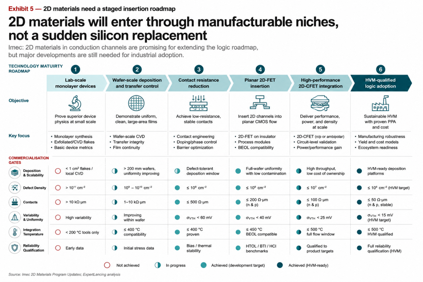
That distinction matters. The winning 2D roadmap will not be the most elegant laboratory result. It will be the one that solves wafer-scale deposition, contact resistance, variability, defect density, integration temperature, and contamination compatibility with existing fabs.
For executives, the right question is not “Will 2D materials replace silicon?” The better question is: Where can 2D materials first create a manufacturable advantage without breaking the process flow?
Wide-Bandgap Materials are Industrializing Beyond the Logic Race
Not all semiconductor materials innovation is about leading-edge logic. Silicon carbide and gallium nitride are reshaping power electronics, particularly in EVs, solar inverters, energy storage, industrial drives, data centers, and fast charging.
Wolfspeed opened its Mohawk Valley 200 mm silicon carbide fab in 2022 and has positioned it as central to the transition from silicon to SiC power devices [Wolfspeed]. By June 2024, the company reported progress in ramping 200 mm wafer activity at Mohawk Valley and its materials facilities [Wolfspeed]. STMicroelectronics is also expanding SiC capacity, including a high-volume 200 mm SiC manufacturing facility in Catania, and highlights SiC’s advantages in higher voltage, higher frequency, faster switching, lower losses, and better thermal management [ST].
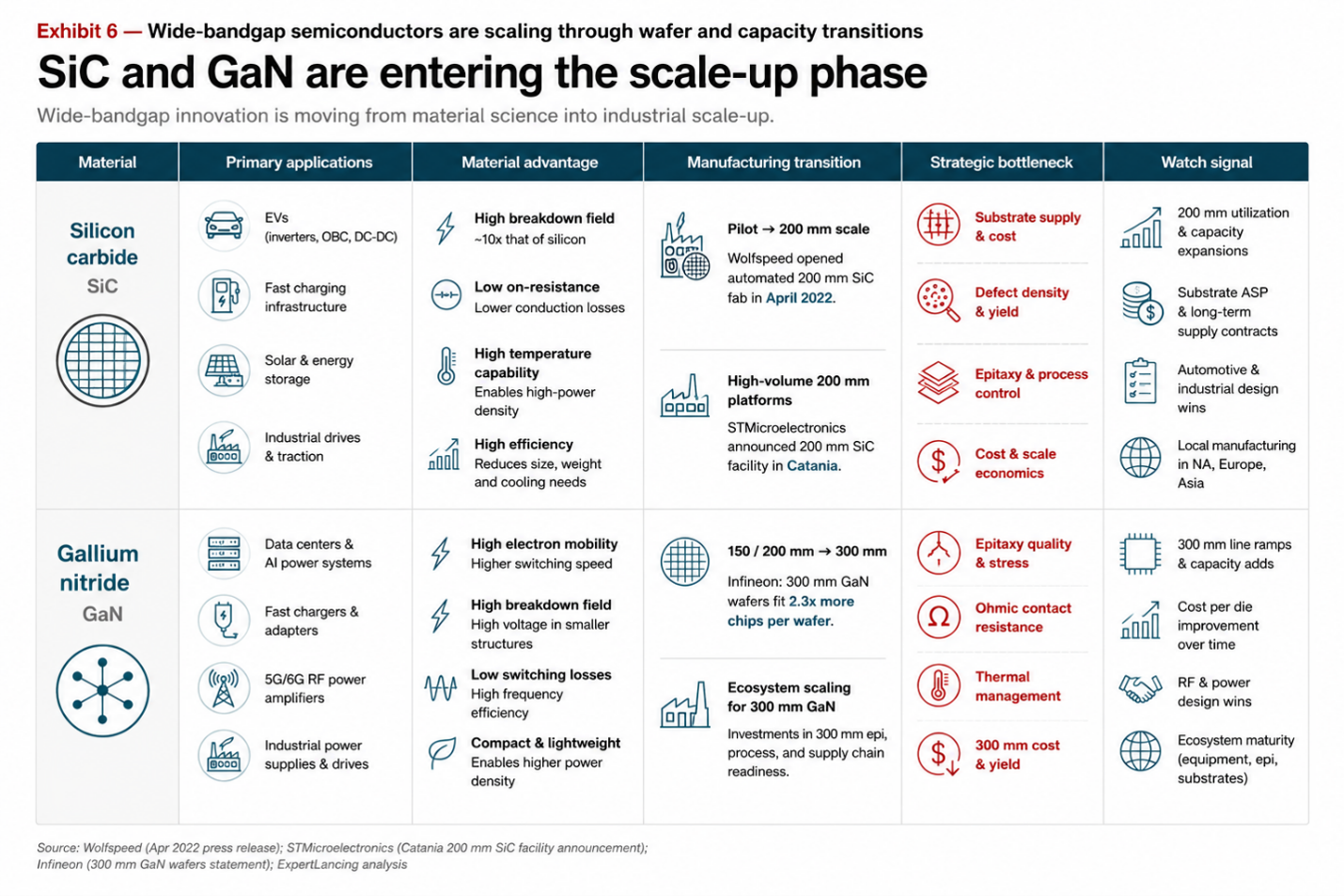
GaN is following a related but distinct path. Infineon announced a 300 mm GaN wafer breakthrough, stating that 300 mm wafers can produce about 2.3 times as many GaN chips as 200 mm wafers, with implications for cost reduction [IEEE, Infineon, ST].
The strategic point is that wide-bandgap semiconductors are not simply “better materials.” They require new substrate strategies, epitaxy know-how, defect control, packaging, qualification, and customer education. Automotive and industrial customers will not adopt them on performance claims alone. They need reliability data, supply assurance, cost curves, and application engineering.
Packaging Materials are Becoming Scaling Materials
Advanced packaging used to sit downstream of front-end innovation. That boundary is dissolving.
AI accelerators, chiplet architectures, HBM integration, and heterogeneous compute have made substrates, interposers, bonding interfaces, underfills, thermal interface materials, and warpage control central to system performance. The material question has moved from “How do we package the chip?” to “How do we make the package part of the chip’s architecture?”
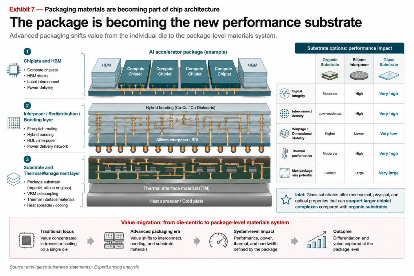
Glass substrates illustrate the shift. Intel has argued that glass substrates can overcome limitations of organic substrates by offering better flatness, thermal and mechanical stability, lower pattern distortion, and much higher interconnect density. It has positioned glass as an enabler for large chiplet complexes and future high-density packages. Samsung Electro-Mechanics has also highlighted glass-core substrates for AI, server, and automotive applications, citing benefits in reduced thickness, warpage improvement, and signal performance.
Hybrid bonding is another signpost. Applied Materials’ 2025 investment in BESI reflected the increasing strategic value of hybrid bonding equipment, which supports direct chip-to-chip bonding for advanced packaging [BESI].
The centre of gravity is shifting. Some of the most valuable materials innovations may no longer sit only inside the transistor. They may sit between chiplets.
Sustainability Pressure will Change Qualification Economics
The industry’s materials roadmap also faces a regulatory and sustainability constraint: fluorinated chemistries, including PFAS.
Semiconductor manufacturing uses fluorinated materials in several critical areas, including lithography, wet chemistry, etch and deposition, CMP, packaging, and emissions-control systems. SIA has convened a PFAS Consortium to develop a science-based understanding of PFAS use and substitution challenges across semiconductor manufacturing.
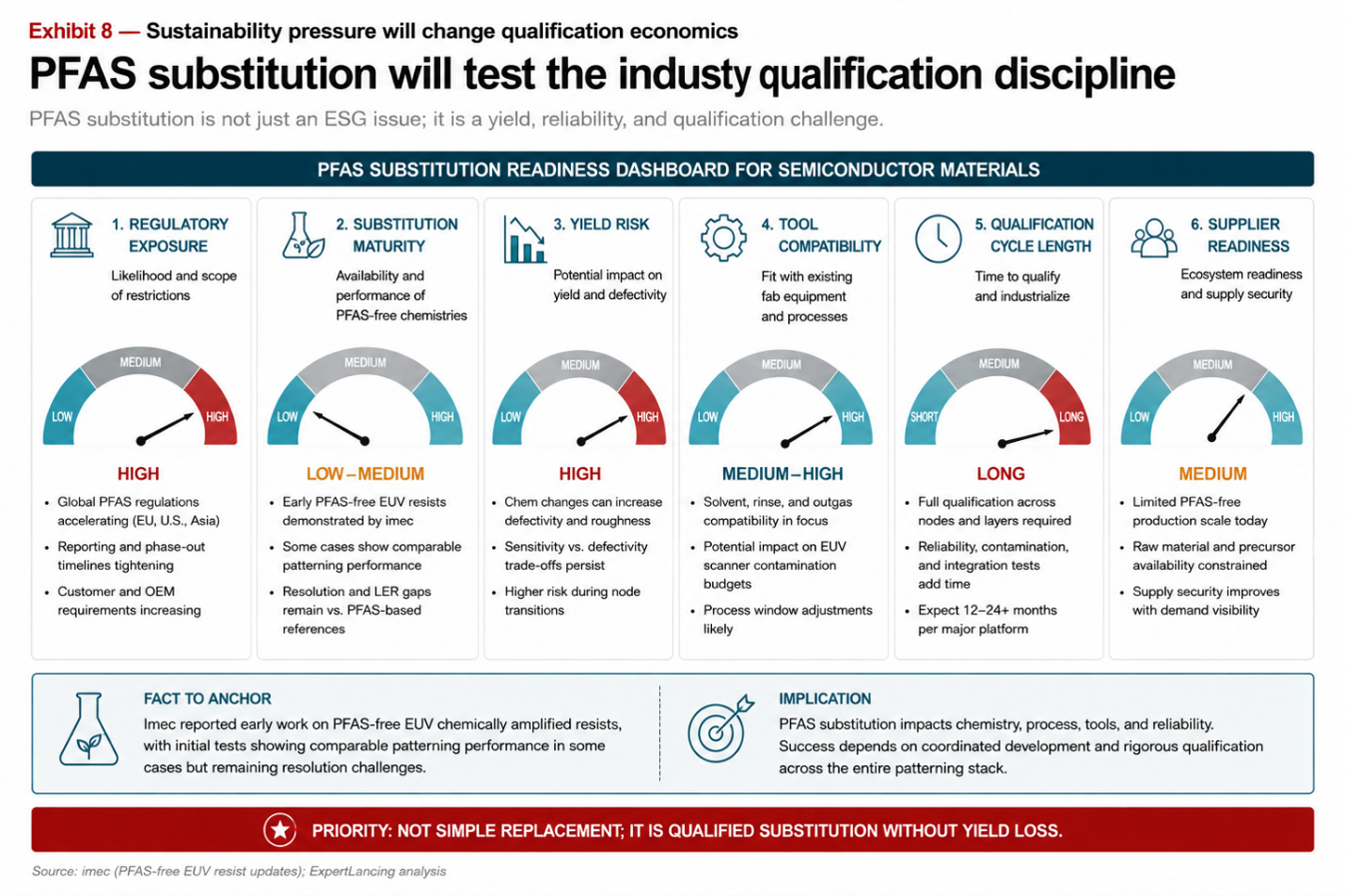
IMEC has reported early progress on PFAS-free EUV photoresists, including chemically amplified resists with comparable patterning behaviour in some cases, while noting remaining resolution and process challenges. It has also pointed out that DUV immersion and broader process-chemistry substitution remain harder problems.
This is not a simple “ban and replace” issue. Semiconductor materials have long qualification cycles because tiny chemical changes can affect yield, defectivity, reliability, and tool compatibility. The companies that win will treat sustainable chemistry as an engineering roadmap, not a compliance exercise.
What Leaders Should Do Next
Semiconductor executives should now treat materials strategy as a board-level capability question.
First, build deeper co-development models with materials suppliers. The old transactional model such as qualify, procure and negotiate price is too slow for High-NA EUV, backside power, hybrid bonding, and PFAS substitution.
Second, map material dependencies by technology node and package architecture. Critical dependencies should include not only wafers and gases, but also resists, underlayers, CMP slurries, electroplating chemistries, thermal materials, substrates, bonding materials, and abatement consumables.
Third, create early-warning systems around regulatory exposure. PFAS, greenhouse gas emissions, water use, and chemical waste will increasingly affect material availability and cost.
Fourth, integrate packaging materials into front-end roadmaps. Chiplet performance cannot be separated from substrate performance, thermal behaviour, and bonding reliability.
Finally, invest in application-specific materials roadmaps. AI accelerators, EV inverters, RF devices, memory, and sensors will not converge on one material stack. The winners will segment by use case and optimize accordingly.
Conclusion: the material stack is strategy
The semiconductor industry has entered a phase where materials innovation is not a supporting act. It is one of the main theatres of competition.
High-NA EUV needs new resist ecosystems. Backside power needs new metallization and dielectric integration. 2D channels need manufacturable insertion paths. Wide-bandgap devices need crystal quality, epitaxy, and packaging maturity. Advanced packaging needs substrates and bonding materials that can scale with chiplet complexity. Sustainable chemistry needs to preserve yield while reducing regulatory risk.
The next generation of semiconductor advantage will not be defined only by who owns the most advanced fab. It will also be defined by who controls, qualifies, and co-optimizes the most critical materials.