
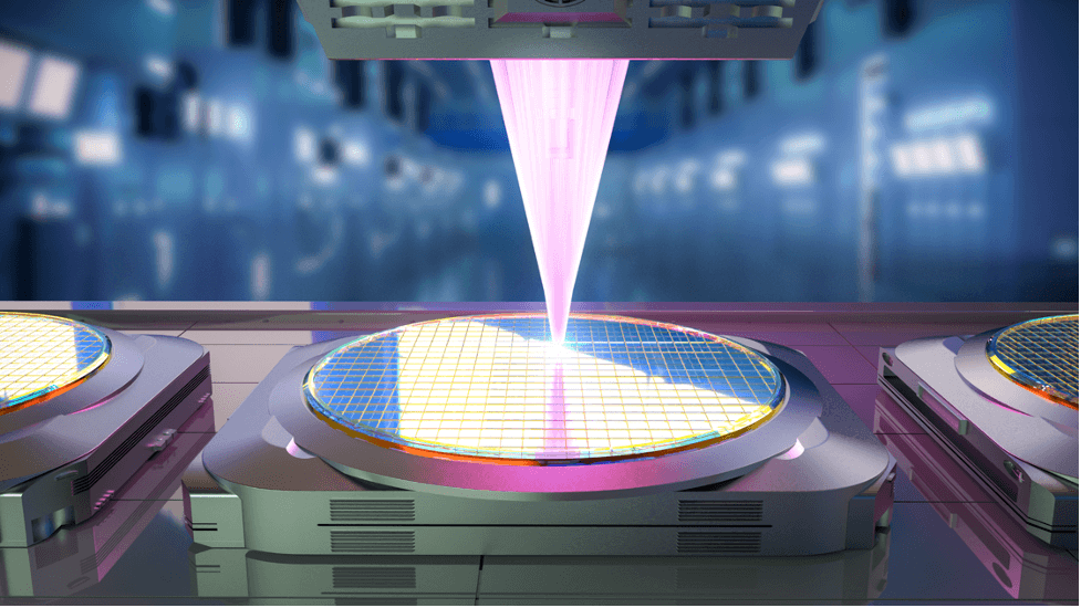
How High-NA EUV is reshaping materials, mask infrastructure, and inspection strategies for reliable sub-3nm semiconductor manufacturing.
Executive Summary
As the semiconductor industry advances beyond the 3nm node, standard 0.33 Numerical Aperture (NA) Extreme Ultraviolet (EUV) lithography hits its physical limits. To avoid the punitive costs and cycle-time penalties of EUV double-patterning, leading-edge logic and memory fabs are transitioning to High-NA (0.55 NA) EUV. This transition is not merely a swap of projection optics; it is a violent disruption of the entire materials and inspection ecosystem.
Executive Takeaway
The transition to 0.55 NA EUV fundamentally rewrites the rules of yield management. Because a single unmitigated defect or stochastic failure at sub-3nm dimensions routinely destroys an entire die, yield control is shifting from the fab floor back upstream to the materials and mask-shop level. Investors and strategists must recognize that value capture is migrating toward defect-inspection metrology and novel materials chemistry.
This whitepaper outlines the cascading effects of the 0.55 NA transition, identifying where defectivity risk concentrates and how value will be captured across the photoresist, pellicle, and actinic inspection markets in the 2025–2030 timeframe.
1. High-NA EUV: Technology Transition and Manufacturing Economics
The physical imperative for High-NA EUV is governed by the Rayleigh criterion for resolution (CD):

To achieve 8nm resolution at a 13.5nm wavelength (λ), platforms like the TWINSCAN EXE:5000 from ASML increase the NA from 0.33 to 0.55. However, the larger angles of incident light required by a 0.55 NA system mandate the use of anamorphic optics mirrors that magnify differently in the X (4x) and Y (8x) axes. This optical shift halves the exposure field from the traditional 26 mm × 33 mm down to 26 mm × 16.5 mm.
The Capital vs. Return Calculus
The economics of High-NA adoption are fiercely contested. At an estimated cost exceeding $380 million per scanner, fabs must weigh immense capital expenditure against the operational returns of avoiding EUV double-patterning.
Single-exposure High-NA reduces cycle times, eliminates overlay errors inherent in multi-patterning, and cuts overall fab energy consumption. However, the half-field size necessitates faster reticle and wafer stages, increasing mechanical complexity and fundamentally altering mask-blank utilization logic for top-tier foundries like TSMC, Intel, and Samsung Electronics.
Key Statistics: High-NA EUV Economics
- System Cost: ~$380M–$400M per scanner.
- Resolution: 8nm (enabling 2.9x higher transistor density than NXE systems).
- Throughput Target: >150 Wafers Per Hour (WPH) at 50 mJ/cm² dose.
- Initial HVM Insertion: Targeting 2025–2026 for sub-2nm logic and advanced DRAM.
2. Photoresist Requirements for High-NA EUV
At sub-3nm dimensions, lithography is no longer just about printing a line; it is about managing the statistical probability of photons striking the resist. This phenomenon, known as photon shot noise, leads to stochastic defects, random micro-bridges or broken lines caused by uneven photon distribution.
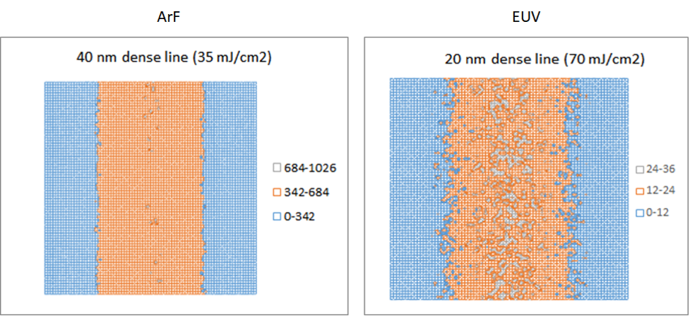
Stochastic Origins of EUV Feature Edge Roughness. Source: SemiWiki
The Limits of CAR and the Rise of MOR
For decades, the industry relied on Chemically Amplified Resists (CAR), originally pioneered by companies like Tokyo Ohka Kogyo (TOK) and Fujifilm Electronic Materials. In CAR, a single photon generates an acid that catalyzes multiple chemical reactions. At 0.55 NA, the diffusion of this acid (acid blur) exceeds the allowable Line-Edge Roughness (LER) budget.
The value chain is heavily shifting toward Metal Oxide Resists (MOR), spearheaded by Inpria, now a subsidiary of JSR Corporation. MOR utilizes direct metal-oxygen bond cleavage. Because the organometallic molecular building blocks (often tin-oxide cores) are significantly smaller and heavier than CAR polymers, MOR offers superior EUV photon absorption and dramatically higher etch resistance, enabling thinner resist films that prevent pattern collapse.
Strategic Implications: The Dose Trade-Off
The transition to MOR is not free. While they solve the LER and etch resistance problems, they traditionally require a higher “dose-to-size” (lighter). This forces scanners to run slower, impacting fab throughput unless the EUV source power is aggressively scaled.
3. Pellicles and EUV Mask Infrastructure
A photomask in an EUV scanner sits at the focal plane. Without a pellicle (a protective membrane), any airborne particle falling on the mask will print directly onto the wafer, destroying the die.
The Carbon Nanotube (CNT) Imperative
Standard 0.33 NA EUV systems operate at roughly 250W to 350W source power. High-NA systems, to maintain throughput with half-field reticles and dose-heavy MOR resists, require source powers scaling from 600W to 1,000W.
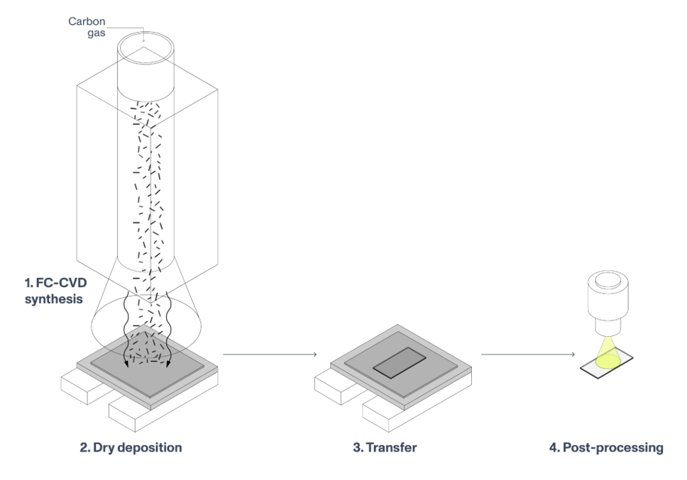
CNT Membrane Fabrication Process. Source: Canatu
At these extreme thermal loads, traditional polysilicon pellicles degrade or melt. The industry is urgently pivoting to Carbon Nanotube (CNT) pellicles, which can survive extreme temperatures while maintaining the required >94% EUV transmission rates.
To meet the 2025–2026 High-NA adoption wave, strategic partnerships are forming to commercialize this technology at scale. Most notably, in late 2023, the leading nanoelectronics research center imec and Japanese chemical leader Mitsui Chemicals signed a strategic partnership to integrate imec’s fundamental CNT pellicle innovations into Mitsui’s manufacturing lines to achieve full production specifications for >600W systems.
Multi-Layer Mask Blank Constraints
EUV mask blanks, supplied by leaders like HOYA and AGC, consist of 40 to 50 alternating layers of Molybdenum (Mo) and Silicon (Si). As the High-NA process window shrinks, the tolerance for multi-layer mask blank defects drops to absolute zero, placing immense pressure on blank suppliers to deliver flawless raw materials.
4. Actinic Mask Inspection for High-NA EUV
As feature sizes shrink, conventional Deep Ultraviolet (DUV) and electron-beam mask inspection tools supplied by KLA and Applied Materials become functionally blind to the most insidious threat: phase defects buried within the Mo/Si multilayer.
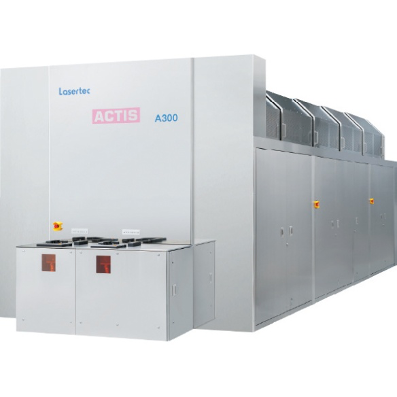
Lasertec ACTIS A300 Inspection System. Source: Lasertec
Because EUV optics rely on reflection rather than transmission, a defect inside the mirror layers might not look like an anomaly to a DUV tool, but it will scatter 13.5nm light and print a defect on the wafer.
The Strategic Role of 13.5nm Inspection
Actinic Patterned Mask Inspection (APMI) tools, most notably the ACTIS A300 series from Lasertec use the exact same 13.5nm EUV wavelength as the scanner itself. This is the only reliable way to guarantee that a reticle is defect-free before it enters production.
High-NA exacerbates inspection challenges in two primary ways:
- Anamorphic Detection: The inspection tool must mimic the scanner’s anamorphic optics, requiring different resolution sensitivities in the X and Y axes to accurately predict defect printability.
- Curvilinear Mask Data: To maximize the process window, High-NA designs heavily rely on Inverse Lithography Technology (ILT), which produces complex, curvilinear mask shapes. Validating these organic shapes via Die-to-Database (DDB) inspection requires massive computational overhead and significantly extends processing time.
Technology Watch: AMI is the Ultimate Bottleneck
AMI is transitioning from a luxury QA step to an absolute bottleneck necessity. Fabs and mask shops that fail to secure actinic inspection capacity will face insurmountable yield walls at the 2nm node and beyond.
5. Implications for the Semiconductor Supply Chain
The shift to High-NA EUV redistributes power across the semiconductor supply chain. Investors and strategic planners should structure their risk models around the following value-capture realities:
- Inspection Becomes the Gatekeeper: As defect tolerances approach zero, metrology and inspection providers capture disproportionate value. Actinic inspection is no longer just a mask-shop tool; its deployment will increasingly pull into the fab itself to monitor pellicle degradation over time.
- The Materials Premium: The transition from CAR to MOR represents a generational reset in the photoresist market. Incumbents must adapt to metal-oxide chemistries, or risk ceding the high-margin sub-3nm market to specialized challengers.
- Consolidation in Mask Infrastructure: The capital intensity required to produce zero-defect mask blanks and >94% transmission CNT pellicles is forcing consolidation. Lead times for these consumables will stretch, and suppliers who can guarantee scale and capacity in the immediate future hold immense pricing leverage.
Conclusion
High-NA EUV marks a fundamental shift in semiconductor manufacturing, where yield leadership depends as much on advanced materials and inspection as on lithography itself. As defect tolerances approach zero, metal oxide resists, CNT pellicles, ultra-low-defect mask blanks, and actinic inspection become essential enablers of sub-3nm production. Between 2025 and 2030, the greatest value will be captured by companies that can deliver these technologies at production scale while enabling higher yield and lower manufacturing risk.