
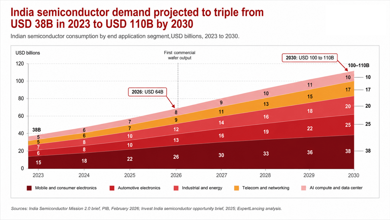
India semiconductor investment is no longer a policy promise; it is becoming a live test of the country’s broader semiconductor ecosystem. The conventional wisdom on India’s semiconductor ambition, as recently as 2023, was that it was a subsidy-chasing exercise destined to fail. Vedanta and Foxconn’s USD 19.5 billion joint venture collapsed in July 2023. The Adani Group’s discussions with Israel’s Tower Semiconductor paused in April 2025. Critics pointed to these setbacks as evidence that India lacked the industrial fabric, water and power infrastructure, and tier-one supplier ecosystem to host a credible fab cluster.
That reading is now obsolete. As of December 2025, India had ten approved semiconductor projects representing total committed investment of approximately INR 1.60 lakh crore, with the Minister for Electronics and IT confirming committed investments approaching USD 90 billion and a working ceiling that could approach USD 150 billion as artificial intelligence infrastructure decisions accelerate through 2026. The list of committed players is no longer speculative. It includes Micron, which began commercial output at its USD 2.75 billion Sanand ATMP facility in early 2026. Tata Electronics, in technology partnership with Taiwan’s Powerchip Semiconductor Manufacturing Corporation, is building India’s first commercial wafer fab in Dholera at a planned 50,000 wafers per month for 28nm to 110nm logic and analog nodes. Applied Materials has committed USD 400 million over four years to a Bengaluru engineering center with potential to support more than USD 2 billion in downstream activity. Lam Research, KLA, CG Power with Renesas and Stars Microelectronics, Kaynes Semicon, Tata Assembly and Test in Assam, and a growing list of OSAT and ATMP India players have followed.
We think the consensus framing of India’s chip story as a “national industrial policy success” is too narrow. The commitments are not primarily a response to Indian subsidies. They are a response to three structural bets that global semiconductor players are placing simultaneously: a geopolitical bet on supply chain resilience, a talent bet on the world’s largest design engineering pool, and a demand bet on the third-largest electronics consumption market by 2030. Understanding which bet drives which player is the key to predicting which commitments will scale and which will retrace.
The Geopolitical Bet Behind India’s Semiconductor Investment Growth
The most underappreciated driver of India’s semiconductor commitments is not only what India offers, but what the rest of the map increasingly does not. US export controls on advanced semiconductor equipment to China, escalating since the October 2022 Bureau of Industry and Security rules and reinforced through 2024 and 2025, have materially constrained China’s viability for advanced-node expansion by multinational semiconductor players. Taiwan’s geopolitical risk premium, however priced, remains non-zero. Vietnam, Malaysia, and Thailand offer strong assembly and test capabilities but lack the scale, domestic demand profile, and broader ecosystem depth required to anchor frontier semiconductor capacity in the AI era. This is why India is increasingly being evaluated through the lens of semiconductor supply chain resilience.
This increasingly positions India as the largest democratic geography outside the established US-Taiwan-Korea-Japan semiconductor corridor with the scale, engineering talent, English-language operating environment, and policy commitment required for long-term ecosystem expansion. The China Plus One thesis, often invoked loosely, has measurable substance in semiconductors. Foxconn’s expanding electronics manufacturing footprint in India through 2024 and 2025, particularly in support of large-scale iPhone production, has contributed to the supplier ecosystem density required for semiconductor packaging and test operations. The flow of commitments from equipment ecosystem players such as Applied Materials, Lam Research, and KLA typically follows that ecosystem density rather than preceding it.
The Talent Bet: 20 Percent of the Global Semiconductor Design Workforce Already Sits in India
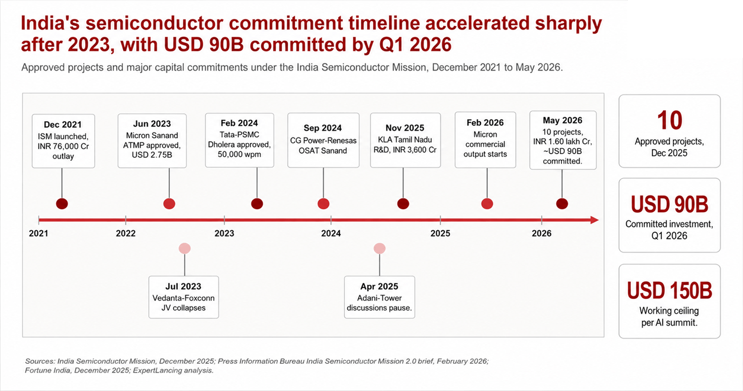
The second structural bet is on talent, and it is the most defensible. India houses approximately 125,000 semiconductor design engineers as of 2025, representing close to 20 percent of the global integrated circuit design. This makes the India semiconductor design workforce one of the strongest foundations for chip design talent in India. Almost every leading fabless and IDM player, Intel, Qualcomm, NVIDIA, AMD, Texas Instruments, Broadcom, Micron, MediaTek, Marvell, NXP, Infineon, Renesas, has operated significant design and R&D centers in Bengaluru, Hyderabad, Noida, and Pune for more than two decades.
This is the critical asymmetry. India did not need to build a design talent base from scratch. It needed to convert an established design talent base into a domestic manufacturing and packaging ecosystem. The shift visible from 2023 onward is precisely that conversion. Applied Materials’ USD 400 million Bengaluru engineering center, announced in 2023 and expanded through 2025, is positioned for collaborative tool development with Indian design houses. KLA’s INR 3,600 crore Tamil Nadu R&D hub, announced in February 2026, applies the same logic in metrology and inspection. Lam Research’s commitments through 2025 follow a similar pattern. These are not assembly facilities. They are upstream engineering investments betting that the next generation of semiconductor equipment IP will be co-developed in India.
The strategic implication is that India’s value capture in the global semiconductor stack will be highest in design services, equipment engineering, and intellectual property licensing, with manufacturing capacity following rather than leading. This inverts the conventional fab-first model that dominated the 2000s and 2010s in Korea, Taiwan, and China.
The Demand Bet: India Will Be the Third-Largest Electronics Consumption Market by 2030
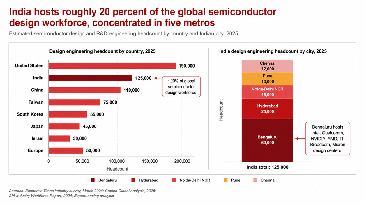
The third bet is on demand. India semiconductor demand is rising alongside the India electronics manufacturing market, electronics manufacturing India, and AI compute infrastructure. The domestic semiconductor consumption is projected to reach approximately USD 64 billion by 2026 and USD 100 billion to USD 110 billion by 2030. The drivers are mobile devices (India is the second-largest smartphone market by units), automotive electronics tied to a passenger vehicle market is approaching 4.7 million units annually and on a trajectory toward 5 million, industrial automation, telecommunications infrastructure for the 5G and emerging 6G rollouts, and a domestic AI compute build-out that the Government of India has identified as a national priority through 2030.
For US, European, Japanese, and Korean semiconductor players, this means India is no longer purely a low-cost manufacturing destination. It is also a strategic end market where local presence affects competitiveness on automotive design wins, telecom infrastructure tenders, and government procurement programs. Micron’s decision to package memory at Sanand, Renesas’s OSAT joint venture with CG Power and Stars Microelectronics targeting 15 million units per day, and Tata Electronics’s Assam assembly and test investment are all positioned to serve domestic Indian demand as a meaningful share of output, not merely export. This is a structural change from the Malaysia and Vietnam OSAT model, where local demand is incidental. It also strengthens the case for semiconductor manufacturing in India as demand shifts from import dependence toward localized supply.
The Incentive Architecture Has Been Restructured to Reduce Player Risk
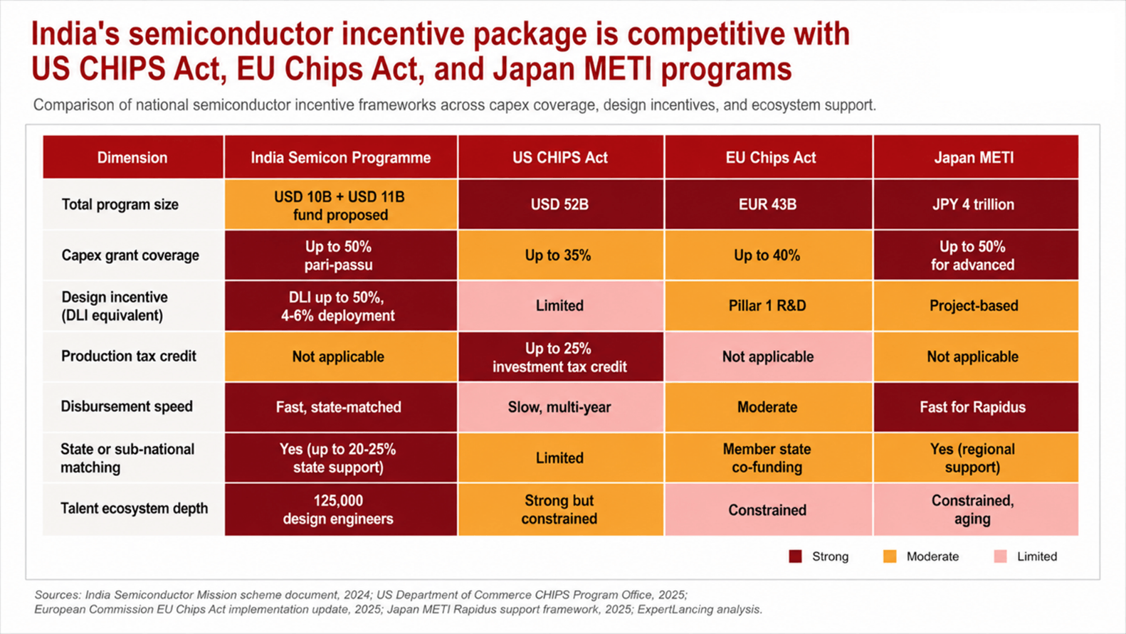
The fiscal architecture matters because it reframes the risk equation for foreign entrants. Under the revised Semicon India programme, the Government of India and state governments jointly fund up to 50 percent of project cost on a pari-passu basis for approved semiconductor fabrication, display fabrication, compound semiconductor, ATMP, and OSAT projects. The Design Linked Incentive (DLI) scheme reimburses up to 50 percent of eligible product design expenditure (capped at INR 15 crore per application) plus a deployment-linked incentive declining from 6 to 4 percent of net sales turnover over five years.
These terms are not unique globally. The CHIPS Act offers comparable headline incentives. What distinguishes India is the speed of disbursement and the political durability across central and state governments. Gujarat, Tamil Nadu, Karnataka, Assam, and Uttar Pradesh have all matched central commitments with state-level land, water, power, and stamp duty concessions. The Vedanta-Foxconn collapse in 2023 and the Adani-Tower pause in April 2025 are instructive: both reflected partner-specific issues, not incentive scheme failures. Projects with credible technology partners and balance sheets, Tata-Powerchip, Micron, CG Power-Renesas, have advanced on schedule.
Risks Are Real and Concentrated in in Semiconductor Fab Execution
A credible thought-leadership view must price the downside. Three risks are concentrated. First, semiconductor fab execution risk: the Tata Dholera plant has reportedly faced schedule slippage on first wafer production, with revised commercial output targets moving deeper into 2026 and 2027. The Dholera semiconductor fab will be a critical test case for whether a large-scale semiconductor fab in India can move from policy approval to commercial yield. India has no precedent for operating a commercial wafer fab at scale; the learning curve on yield, defect density, and equipment uptime will be measured in years, not quarters.
Second, semiconductor infrastructure risk across water and power infrastructure: Dholera and Sanand are situated in water-stressed regions. Long-run capacity expansion will require dedicated ultrapure water and uninterrupted power solutions that are not yet fully built.
Third, geopolitical alignment risk: India’s strategic autonomy posture means it will not align unconditionally with US export controls. This creates ambiguity for advanced-node technology transfer that any prospective sub-14nm fab partner will need to navigate.
Implications for Decision Makers
For global integrated device manufacturers (Intel, Samsung, TSMC, SK Hynix, Texas Instruments, STMicroelectronics, Infineon), the strategic question is whether to enter India through a captive subsidiary, a joint venture, or a technology licensing arrangement. The Tata-Powerchip model has demonstrated that technology partnership without equity exposure is feasible. The next 18 months will determine whether full IDM equity entries become viable.
For fabless and chip design players (NVIDIA, AMD, Qualcomm, MediaTek, Marvell, Broadcom, AMD, ARM), the question is talent retention and design center scale. The 20 percent global workforce share is an asset that competitors are now actively bidding for. Expanding from cost-arbitrage design centers to full-stack product ownership in India is the differentiator.
For semiconductor equipment and materials players (Applied Materials, Lam Research, KLA, Tokyo Electron, ASML, Entegris, Linde, Air Liquide), the question is co-development scale. The early movers have committed; the second wave will need to commit by 2027 or accept disadvantaged positioning when India fab capex enters its second phase.
For Indian conglomerates and infrastructure investors (Tata Group, Adani Group, Reliance, Murugappa, Aditya Birla, JSW), the question is which adjacent layer of the semiconductor value chain offers the highest-return entry. The capital-intensive wafer fab is one option. ATMP, OSAT and ATMP India opportunities, advanced packaging, specialty gases, ultrapure water, fab construction services, and downstream electronics manufacturing services are each significant addressable markets.
For state governments competing for the next wave of investment, the question is differentiation beyond fiscal incentives. Land, water, talent supply, and logistics will increasingly outweigh subsidy stacking in player decisions.
For private equity and infrastructure investors, the question is platform construction in the ecosystem rather than direct fab exposure. OSAT consolidation, semiconductor services, and equipment distribution are the highest-IRR entry points through 2028.
What to Watch in the Next 12 to 24 Months
First, Tata-Powerchip Dholera first wafer production. The shift from trial output to commercial volume, expected in stages through 2026 and 2027, will determine whether India’s wafer fab thesis is structurally validated or requires recalibration. This will also determine how quickly the market validates the semiconductor fab in India thesis.
Second, the second wave of state government project approvals through 2026. The Government of India has signaled intent to expand the ten-project base toward fifteen to twenty approved projects, with a particular focus on compound semiconductors (silicon carbide, gallium nitride) and advanced packaging. New approvals through Q4 2026 will indicate which technology nodes and segments are prioritized.
Third, advanced-node technology transfer arrangements. Any movement on sub-14nm logic or advanced memory in India, whether through TSMC, Samsung, SK hynix, or Intel Foundry, will signal that the global semiconductor industry views India as ready for frontier capacity. Absence of such announcements through 2027 would suggest the ecosystem remains positioned for mature and trailing nodes.
The Vedanta-Foxconn collapse made for compelling 2023 headlines. The Tata-Powerchip ramp, Micron’s Sanand commercial output, and the Applied Materials and KLA upstream commitments are the data points that matter. India’s semiconductor ecosystem in 2026 is not a policy promise. It is a portfolio of executing projects with global player capital, world-class design talent, and the largest non-aligned democratic end market in the world. India semiconductor investment is now being driven by supply chain resilience, chip design talent, domestic demand, and the long-term need for semiconductor manufacturing. The strategic question for global semiconductor leadership is no longer whether to engage with India. It is how late one can afford to be.
For global semiconductor companies, investors, and suppliers, the business takeaway is clear: the India semiconductor ecosystem is becoming too large to ignore, and semiconductor investment in India is moving from optional exposure to strategic necessity.
For semiconductor market entry, investment screening, or supplier ecosystem analysis, connect with ExpertLancing.