
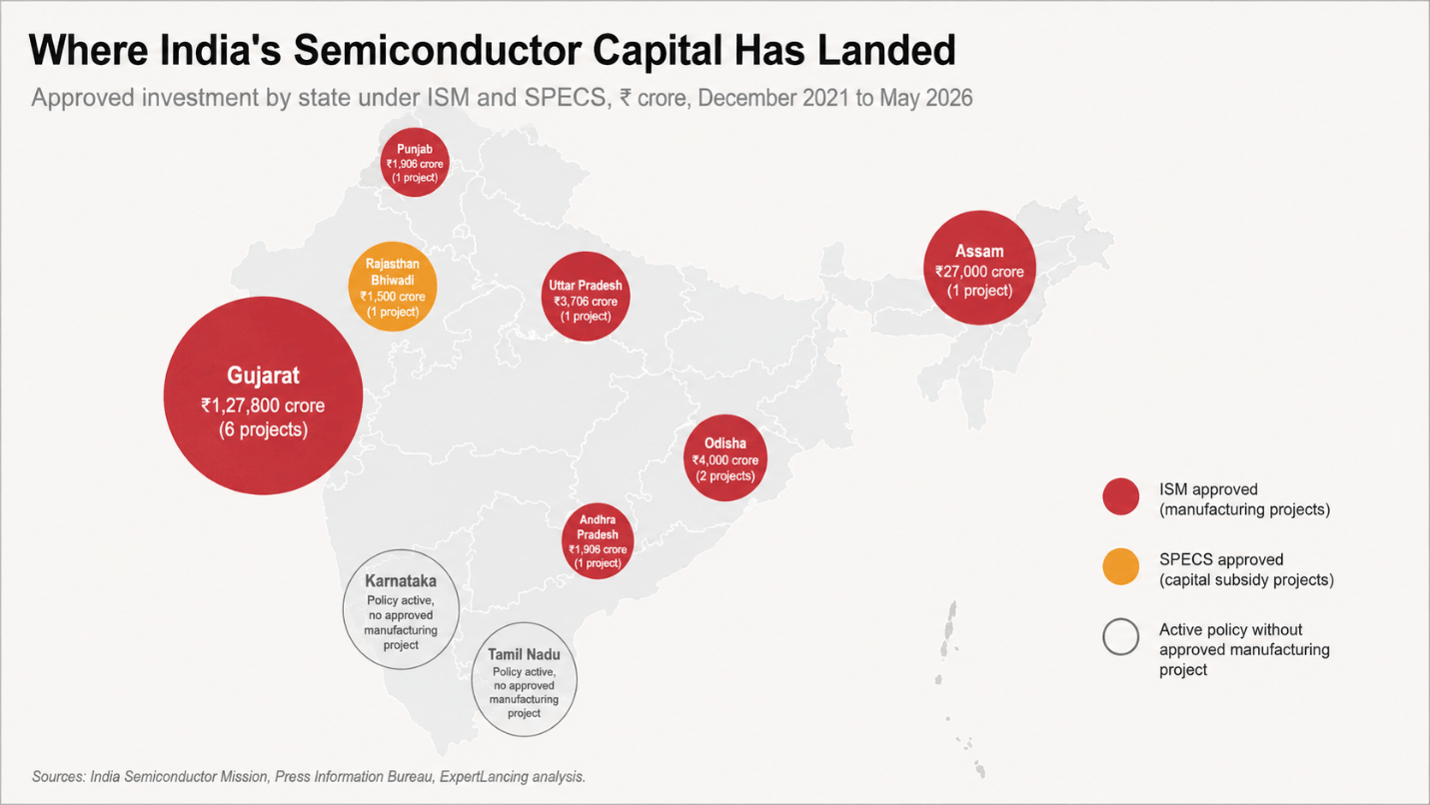
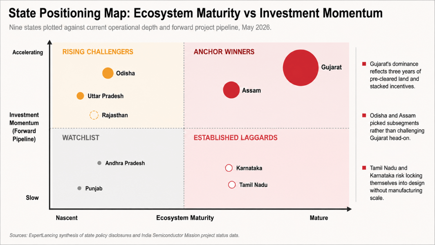
When the Union Cabinet cleared two more semiconductor projects on May 5, 2026, both went to Gujarat. That decision lifted Gujarat’s share of approved facilities under the India Semiconductor Mission to six of twelve, and its share of approved capital to roughly three-quarters of the ₹1.64 lakh crore committed across the program. For readers tracking the India semiconductor race, the latest approvals show how India semiconductor projects are concentrating around a few early movers, especially the Gujarat semiconductor hub. The official storyline names six states as semiconductor destinations. The capital flows tell a different story. India has one runaway leader, one credible second mover, and a chasing pack still searching for a defining anchor project.
For multinational chipmakers weighing India site selection, and for state governments treating chips as a generational industrial prize, state-wise semiconductor investment is the central fact of 2026. The race is happening. It is not yet competitive.
Why Every State Now Cares About Wafers
Three trends collided to make semiconductor capacity a state-government priority rather than only a central one.
First, the global semiconductor supply chain restructured around political risk. Taiwan, South Korea, and mainland China together account for the dominant share of leading-edge fabrication, and the United States, Japan, and the European Union have all moved to onshore or friend-shore capacity through dedicated chip acts since 2022. India’s pitch is geographic and geopolitical insurance, plus a fast-growing domestic demand base.
Second, the demand math is unusually durable. India’s semiconductor market has grown from $38 billion in 2023 to $45 to $50 billion in 2024 to 2025 and is projected to reach $100 to $110 billion by 2030. Government policy explicitly targets 70 to 75 per cent self-sufficiency in domestic chip demand by 2029, with longer-horizon ambitions on advanced nodes.
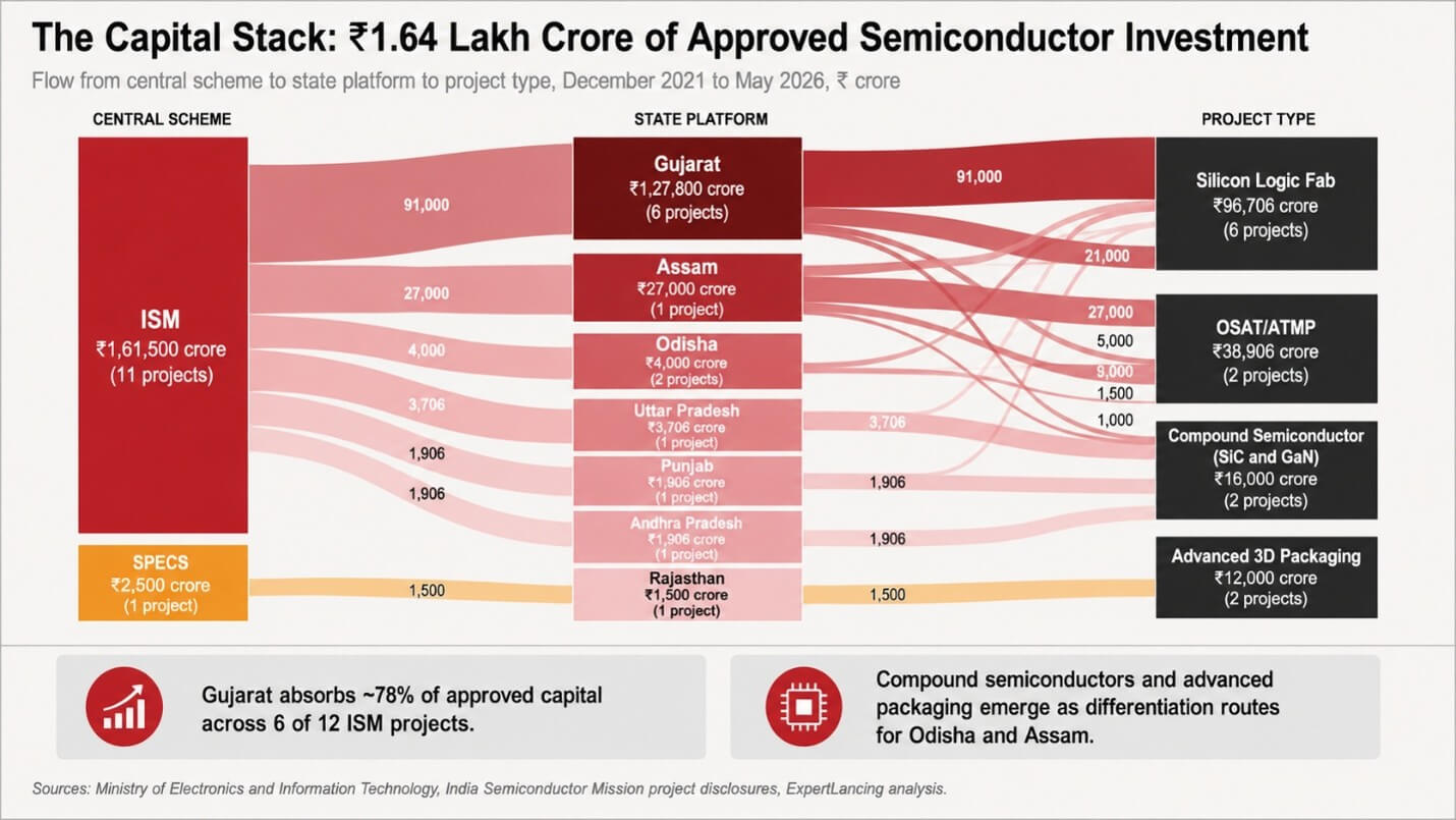
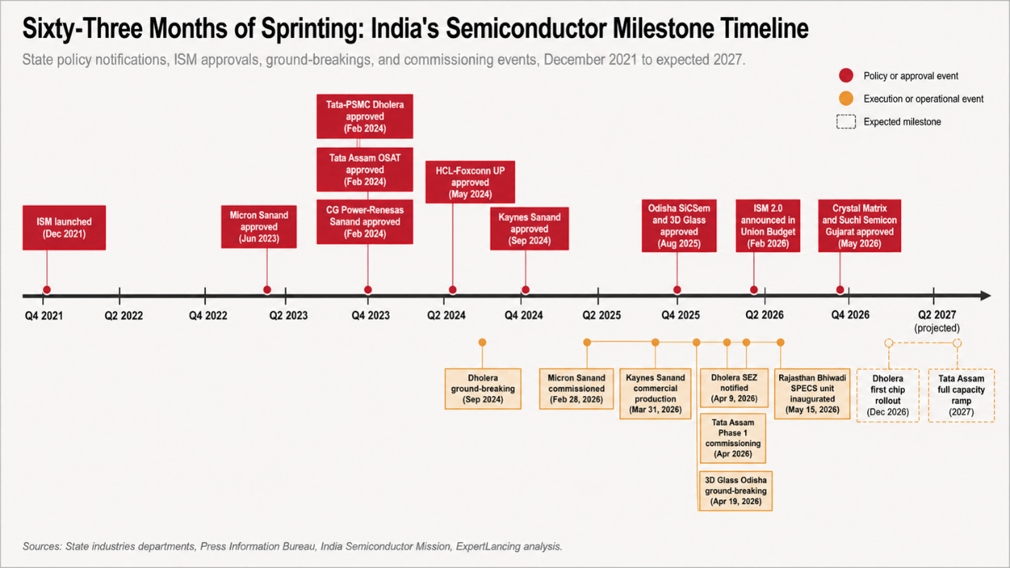
Third, the central scheme architecture invited state participation by design. The India Semiconductor Mission was approved in December 2021 with an incentive outlay of ₹76,000 crore and fiscal support of up to 50 per cent for silicon fabs, compound semiconductor facilities, assembly and testing units, and chip design. Crucially, applicants must demonstrate state-level commitments on land, power, water, and matching incentives. That clause turned every state with industrial ambition into an active bidder.
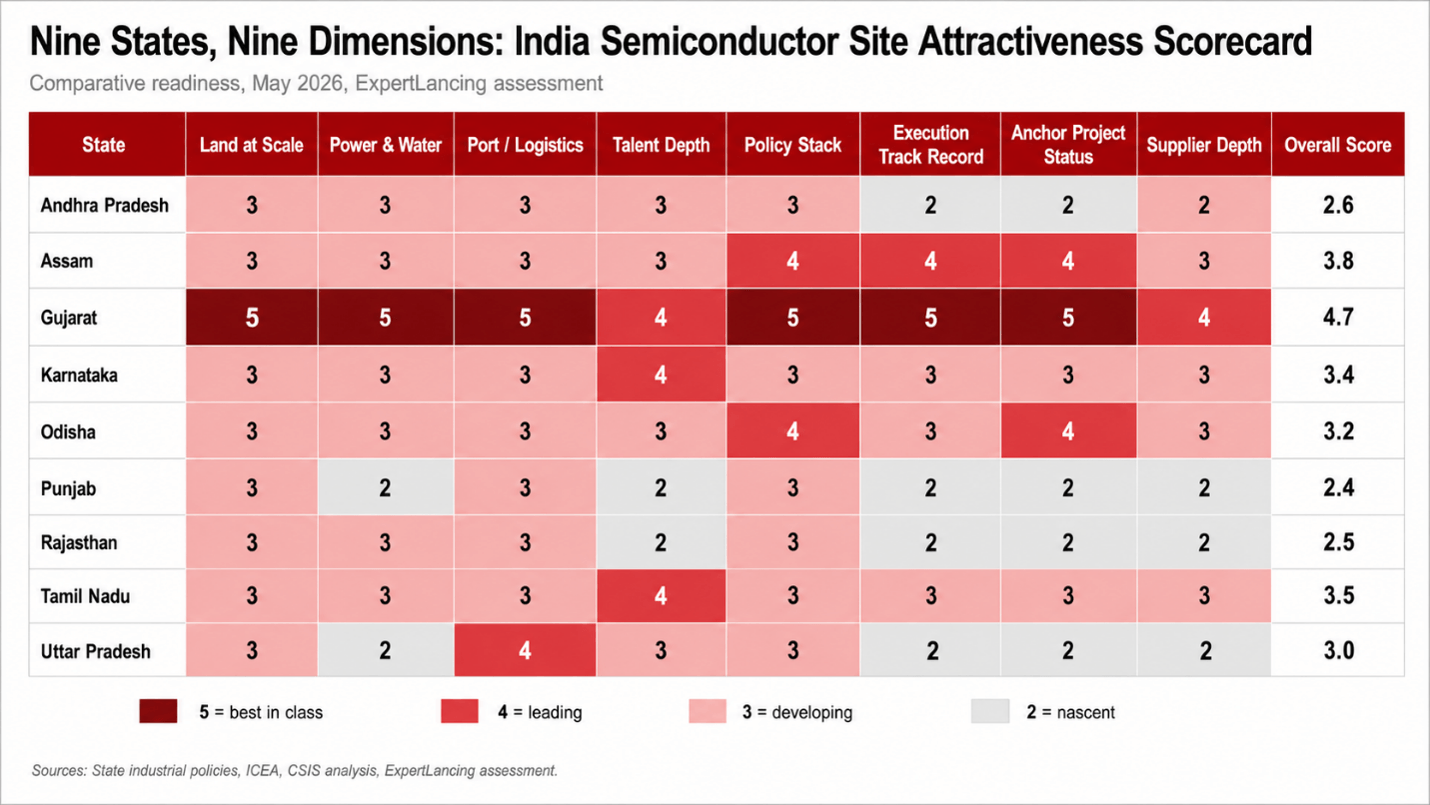
The 4-3-2-1 Scoreboard
As of May 2026, the active state ranking is unambiguous. The current map of India Semiconductor Mission projects shows why searches for India semiconductor projects by state increasingly start with Gujarat.
| State |
Number of Projects/Positions |
Key Anchor Project | |
| Gujarat | 4 major ISM-approved projects, with six approved facilities overall | Tata Electronics and PSMC Dholera semiconductor fab, plus Sanand packaging units | |
| Assam | 1 major second-mover project | Tata semiconductor assembly and testing project at Jagiroad | |
| Odisha | 2 approved projects | SiC semiconductor facility and 3D Glass Solutions ATMP plant in Bhubaneswar | |
| Uttar Pradesh | 1 approved project | HCL-Foxconn semiconductor assembly and testing facility in Jewar | |
| Rajasthan | 1 non-ISM semiconductor unit | ATMP/OSAT facility in Bhiwadi under SPECS | |
| Tamil Nadu and Karnataka | No approved manufacturing | Design, equipment, and policy-led semiconductor ecosystem development |
Of the 12 approved projects, four are in Gujarat, three of them in Sanand alone. Gujarat’s anchor is the Tata Electronics and Powerchip Semiconductor Manufacturing Corporation (PSMC) fab in Dholera. This Dholera semiconductor fab is the centrepiece of semiconductor investment Gujarat and the strongest proof point for Gujarat’s lead. The Tata Group has secured approximately 160 acres in Dholera to establish the nation’s first mega semiconductor fab plant, investing Rs 91,000 crore, with the joint venture beginning by manufacturing 28-nanometer chips. As of April 2026, the Tata-PSMC plant had reached approximately 50 per cent civil completion, with trial production expected by late 2026. Sanand layers in three operational or near-operational packaging units: Micron Technology’s $2.75 billion ATMP facility, inaugurated February 28, 2026, the CG Power, Renesas, and STARS Microelectronics OSAT, and Kaynes Semicon’s OSAT, which began commercial production on March 31, 2026.
Assam is the second mover, and a meaningful one. The Tata semiconductor project in Assam is being developed with an investment of Rs 27,000 crore and is expected to produce 48 million semiconductor chips per day upon completion. The first phase of the plant is expected to be commissioned by April 2026, generating around 15,000 direct and 11,000 to 13,000 indirect jobs.
Odisha, Uttar Pradesh, Punjab, and Andhra Pradesh share the remaining slots. In Bhubaneswar, Odisha, a ₹2,066 crore assembly and testing facility is being set up by SICEMM Private Limited to produce silicon carbide-based diodes and MOSFETs, and a ₹1,943 crore ATMP plant by 3D Glass Solutions Inc. carries investments from Intel, Lockheed Martin, and other venture and private equity funds. Uttar Pradesh hosts the HCL and Foxconn INR 37.06 billion semiconductor assembly and testing facility in Jewar, which will manufacture display driver chips used in smartphones, laptops, PCs, and automotive systems. Rajasthan joined the list outside ISM: an ATMP/OSAT facility in Bhiwadi inaugurated on May 15, 2026, under the Scheme for Promotion of Manufacturing of Electronic Components and Semiconductors, the first semiconductor unit established outside ISM.
Two large industrial states are conspicuously absent from the approved project list: Tamil Nadu, India’s electronics manufacturing leader, and Karnataka, the country’s design capital.
What Gujarat Got Right Three Years Before Anyone Else
Gujarat’s lead reflects three structural choices made before competitors fully understood the contest.
The first is land at scale, pre-cleared. The Dholera Special Investment Region, conceived more than a decade ago along the Delhi-Mumbai Industrial Corridor, gave Tata Electronics a 160-acre footprint inside a state-managed master plan. On April 9, 2026, the government notified Special Economic Zone status for Tata Electronics’ Dholera fab site, a 66-hectare facility with an on-site inland container depot. Sanand’s GIDC industrial estate offered comparable readiness for the three packaging units. No other state currently fields land parcels of this scale that combine pre-built power, water, and customs infrastructure with notified SEZ status.
The second is execution speed. Civil construction of the Tata-PSMC fab reached 45 per cent completion by February 2026, aligning with the Gujarat government’s commitment to ensure all core infrastructure in the region is ready by June 2026. The cargo terminal of the upcoming Dholera airport is targeted for June 2026 operations. The state’s track record of converting cabinet approval into ground-breaking inside twelve to eighteen months has compressed investor risk in a sector where most other emerging-market peers measure delays in years.
The third is policy stacking. Gujarat’s semiconductor policy permits applicants to combine central ISM benefits with state-level capital subsidies, stamp duty waivers, electricity duty concessions, and training reimbursements. Government subsidies from both central and state authorities are anticipated to cover up to 70 per cent of the project expenses for the Dholera facility. Few global manufacturing sites currently offer that cumulative subsidy intensity outside the United States CHIPS Act jurisdictions.
The Chasing Pack – Differentiation, Not Imitation
The smarter laggard states are not trying to outbid Gujarat on the marquee fab. They are picking subsegments.
Odisha has bet on compound semiconductors. On August 12, 2025, SiCSem Private Limited’s silicon carbide fab in Bhubaneswar was approved as India’s first commercial SiC compound semiconductor fabrication facility, with Clas-SiC Wafer Fab Ltd. of the UK as technology partner. Silicon carbide and gallium nitride matter disproportionately to electric vehicles, fast chargers, and grid power electronics, all sectors in which India’s domestic demand is rising faster than the global average. The state’s 2023 policy supports manufacturing and design with up to a 30 per cent capex subsidy, full tax and duty exemptions, concessional land, and funding for very-large-scale integration education and skilling.
Uttar Pradesh has played the proximity card. The HCL and Foxconn project sits next to the upcoming Noida International Airport at Jewar, inside one of India’s densest electronics manufacturing clusters. UP’s 2024 semiconductor policy offers a 50 per cent additional capital subsidy and extensive duty exemptions, though it has yet to attract the volume of projects seen in Gujarat.
Assam’s play is different again. The state is treating Tata’s Jagiroad investment as the seed of a regional industrial ecosystem rather than a single facility. Around 500 women from Assam are being trained in various Tata Electronics facilities, with Tata working with IIT Guwahati and the National Institute of Electronics and Information Technology to develop diploma and certification programmes, building toward an ecosystem of 1,000 suppliers and partners. A satellite electronics city is being built around the plant.
Tamil Nadu and Karnataka, the two states most often cited as natural semiconductor homes, have so far won design and equipment activity but not manufacturing facilities. Under its newly launched Semiconductor and Advanced Electronics Policy 2024, the Tamil Nadu government will offer up to 50 per cent additional financial incentives to semiconductor projects selected under the Centre’s chip subsidy plan, with stamp duty, land and electricity concessions. The state has earmarked roughly 100 acres each for dedicated semiconductor and equipment manufacturing parks at Sulur and near Palladam under the Tamil Nadu Semiconductor Mission 2030. Karnataka is positioning Bengaluru and beyond as a 2-nanometre design and equipment hub: the Karnataka Semiconductor Policy targets over ₹80,000 crore in investment, enabling 2 to 3 fabrication units, and supporting more than 100 design and manufacturing units, with Lam Research committing over ₹10,000 crore for an advanced R&D lab and a semiconductor silicon component manufacturing facility focusing on 2nm technology.
The strategic question for both is whether design talent and equipment investment can substitute for a flagship fab in the next political cycle.
The Incentive Stack: Where the State Layer Actually Matters
Investors do not select states on headline subsidy percentages. They model the stack.
Central support under ISM 1.0 covers up to 50 per cent of project cost. State-level top-ups vary widely: Andhra Pradesh’s 2024 to 2029 policy offers ISM-approved projects a capital subsidy equal to 60 per cent of the central incentive, plus training subsidies. Tamil Nadu offers 50 per cent of the central incentive on top, with stamp duty and electricity concessions. Uttar Pradesh matches with 50 per cent. Odisha offers 30 per cent of capex. Karnataka is finalising its next policy framework.
The differentiators inside that arithmetic are land cost, power tariff, water assurance, and time-to-approval. Gujarat’s GIDC tariffs for high-volume industrial consumers, its dual-port access through Mundra and Kandla, and its single-window clearance system materially compress the effective cost of capital for a five-year build. Gujarat’s ability to provide SEZ notification, GIDC land allocation, and port connectivity through Mundra and Kandla has made it the fastest-executing semiconductor investment destination in the country. Andhra Pradesh and Odisha are building comparable single-window facilitation, but the operational evidence is still thinner.
Who Wins the Decade?
The honest answer is that India’s semiconductor map is still being drawn. Three views shape the next three years.
For investors deciding where to place a first plant, Gujarat remains the lowest-risk choice. The anchor projects are physical, the SEZ status is notified, and the supplier ecosystem is gathering. The trade-off is concentration risk: a single state weather event, labour dispute, or policy reversal would cascade.
For investors entering on the compound semiconductor, advanced packaging, or specialised application route, Odisha, Assam, and Uttar Pradesh now offer credible value propositions backed by approved anchor projects and active state-level execution support.
For investors prioritising design, intellectual property, or equipment manufacturing, Karnataka and Tamil Nadu remain the natural homes despite their thinner manufacturing footprint, especially as ISM 2.0 reweights the central programme. ISM 2.0 was announced in the Union Budget 2026-27 to focus on semiconductor equipment and materials, full-stack Indian semiconductor IP, supply chains, and industry-led research and training centers. If this reorientation lands as drafted, Bengaluru and Chennai become the strategic winners of the next funding cycle even without a new fab.
The honest counterpoint comes from analysts who argue the headline numbers overstate near-term capability. India still imports the bulk of its semiconductor equipment, speciality chemicals, gases, and design IP. The race among states is, in part, a competition for political credit on investments whose true ecosystem value will be measurable only by 2028 or 2029.
What to Watch Through 2027
India semiconductor milestones 2027 will determine whether the country’s chip map becomes genuinely multi-state or remains led overwhelmingly by Gujarat. The most important signal will be the Dholera first chip rollout, followed by Assam’s ramp-up, new ISM approvals, and supplier localisation.
Six milestones will determine whether India’s semiconductor map redraws around multiple anchors or hardens around Gujarat alone.
First, the Dholera first-chip rollout. Union Minister Ashwini Vaishnaw has stated that the first chips from the Dholera plant will be available by December 2026. Delivery on time is the single biggest signal to global customers and to other state governments.
Second, the Assam OSAT ramp. Phase 1 commissioning in April 2026 marks the formal start of commercial-scale chip packaging at Jagiroad, followed by progressive capacity ramp-up through 2026. A successful year-one yield in Jagiroad legitimises the geographic diversification thesis.
Third, Tamil Nadu’s first ISM-approved manufacturing project. None has been announced as of May 2026. A central nod inside the next twelve months would reset the competitive map.
Fourth, the ISM 2.0 detailed scheme guidelines. The incentive support for semiconductor fabrication, OSAT, and ATMP units may be reduced to 30 per cent from 50 per cent in the second phase. Lower subsidy intensity, paired with new categories for equipment and materials, will reshape state-level bidding behaviour.
Fifth, second-fab announcements. The most consequential single event for any non-Gujarat state would be the approval of a second silicon fab in India. UP, Karnataka, Tamil Nadu, and Maharashtra have each signalled bids.
Sixth, supplier and equipment localisation contracts. The race to host fabs is partially won. The race to host the supplier base around them has barely begun.
Conclusion
India’s semiconductor race will look very different by 2028. The early lead has gone to the state that built the runway first and converted approvals into physical infrastructure fastest. The states that will matter in the next round are those that absorb three lessons from Gujarat’s playbook: pre-clear land at industrial scale, stack incentives credibly with central support, and treat execution speed as the primary competitive variable.
For boards of global semiconductor companies, the message from India in May 2026 is direct. The country is open for capacity at terms few jurisdictions can match. The address, today, is overwhelmingly Gujarat. The question for every other state is whether the next eighteen months produce the anchor project that finally turns a one-state story into a national one.
For decision makers, the business takeaway is clear: India semiconductor projects by state should be evaluated not only by subsidy announcements, but also by land readiness, execution speed, supplier depth, talent availability, and long-term policy stability. ExpertLancing helps companies assess semiconductor site-selection choices, compare state-level investment incentives, and build evidence-backed India market-entry strategies for the next phase of the India semiconductor race.