
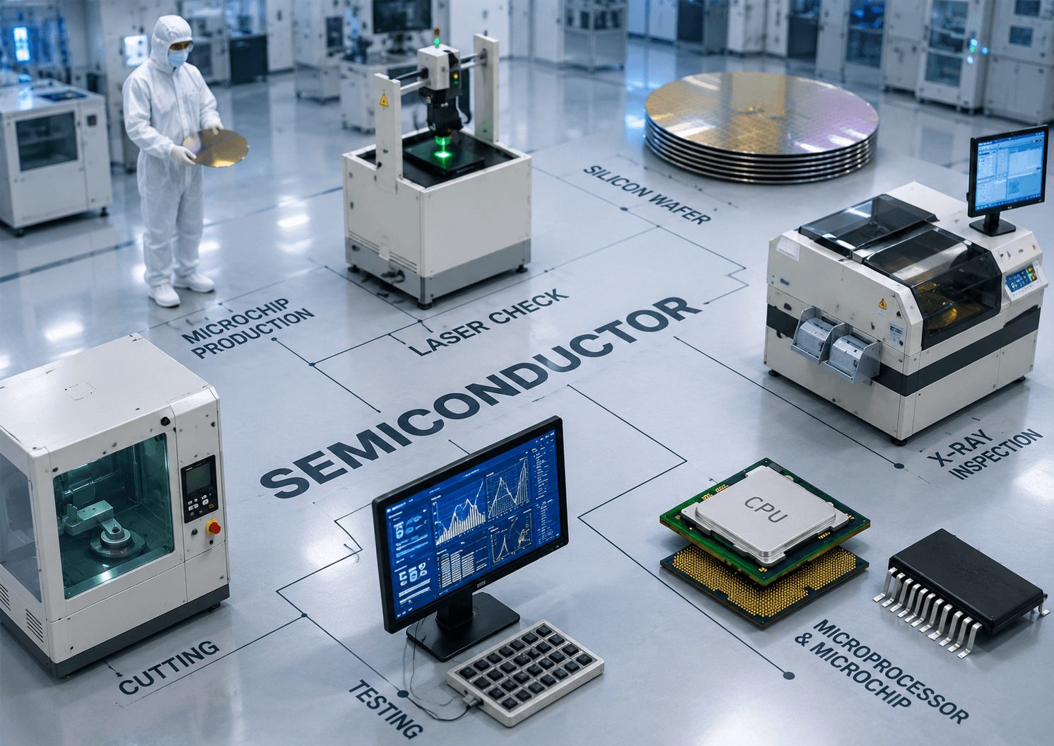
While global attention is focused on India’s high-profile semiconductor fabrication announcements, a quieter but equally important transformation is happening across the country. Beyond the new wafer fabrication plants and government press conferences, there is a critical ecosystem of semiconductor materials, semiconductor equipment, and EDA tools in India that will ultimately determine whether India’s semiconductor goals become a lasting success. This less-discussed area represents both the biggest opportunity and the most urgent challenge for India to become a global semiconductor hub. In other words, the future of the semiconductor supply chain in India depends not only on fabs, but also on the materials, tools, equipment, and design infrastructure that make chip production possible.
The Invisible Infrastructure Powering India’s Chip Dreams
India’s semiconductor market is projected to reach $108.4 billion by 2030, expanding from approximately $49.8 billion in 2025 at a compound annual growth rate of 16.8%. This growth trajectory is impressive, yet the underlying supply chain realities reveal a more nuanced picture. India currently manufactures less than 1% of the world’s semiconductors and relies on imports for approximately 85% of its domestic requirements. The country contributes 20% of global semiconductor design talent, creating a peculiar asymmetry where intellectual capability substantially exceeds manufacturing capacity.
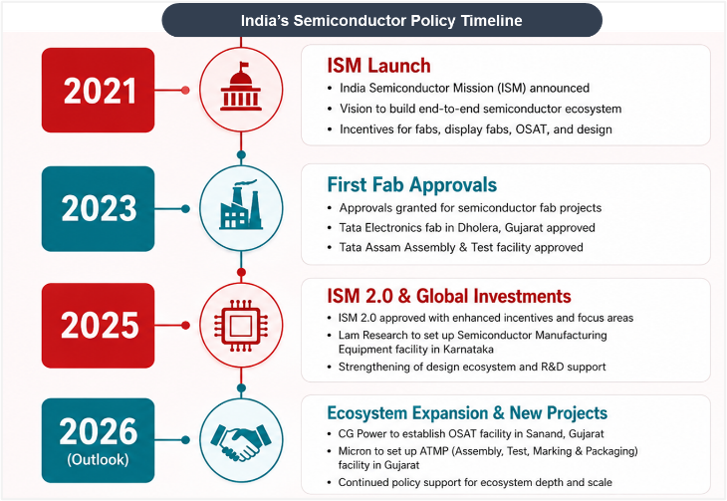
The India Semiconductor Mission, launched with an outlay of INR 76,000 crore (approximately $10 billion), has fundamentally reoriented the policy landscape. The Production Linked Incentive scheme offers fiscal support covering up to 50% of project costs for semiconductor fabs, display fabs, and compound semiconductor facilities. However, the more recent India Semiconductor Mission 2.0, announced in the Union Budget 2026-27 with a provision of Rs. 1,000 crore, signals a maturation in strategic thinking. This iteration explicitly prioritizes producing semiconductor equipment and materials within India, developing full-stack Indian semiconductor intellectual property, and fortifying both domestic and global supply chains.
Materials: The High-Purity Challenge
The semiconductor materials India ecosystem presents a paradox of potential and constraint. The country possesses a robust chemical manufacturing industrial base that manufactures several bulk and specialty chemicals, including acids, solvents, and industrial gases. Yet these products currently lack the ultra-high purity required for semiconductor fabrication, where contamination must be measured in parts per billion or even parts per trillion.
Critical materials required for semiconductor manufacturing include:
- Silicon wafers
- Photoresists
- Ultrapure water
- Hydrogen peroxide
- Etching chemicals
- Industrial gases
The list of critical materials required for semiconductor manufacturing is extensive and technically demanding. Silicon wafers, photoresists, ultrapure water, high-purity hydrogen peroxide, and specialized etching chemicals form the foundation of fabrication processes. Currently, India relies predominantly on suppliers from Japan, South Korea, the United States, and Germany for these inputs. This concentration creates supply chain vulnerabilities that have been exposed during recent geopolitical disruptions, including trade disputes between Japan and South Korea and the Russia-Ukraine war’s impact on neon gas supplies.
Indian chemical companies are beginning to address these gaps. Tata Chemicals is scaling up capabilities to produce high-purity chemicals specifically for etching and cleaning stages in semiconductor manufacturing. Polymatech Electronics, an indigenous opto-semiconductor manufacturer, has acquired Nisene Technology Group in California and signed memoranda of understanding with Japanese firms like Orbray to develop silicon carbide and sapphire wafer capabilities. These developments indicate that Indian enterprises recognize the strategic imperative of vertical integration into the semiconductor materials value chain.
The transition from bulk chemicals to semiconductor-grade materials requires substantial capital investment, sophisticated quality control systems, and rigorous environmental compliance frameworks. The production of photoresists and ultrapure chemicals demands facilities with contamination controls that exceed standard industrial specifications. India must develop specialized logistical supply chains capable of handling volatile, toxic, and ultra-high-purity materials while maintaining stringent environmental safeguards.
Equipment: Building the Tools That Build Chips
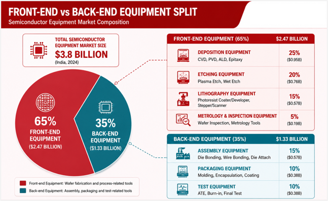
The semiconductor manufacturing equipment market India reached approximately $3.8 billion in 2025 and is projected to grow to $7.7 billion by 2034. This segment is bifurcated between front-end equipment, which constitutes approximately 65% of market volume, and back-end equipment for assembly, testing, and packaging. Wafer fabrication equipment is especially important because it supports core fab processes such as deposition, etching, lithography, cleaning, and metrology.
The most significant recent developments in India’s equipment ecosystem involve major global players establishing substantial presences in the country. Lam Research, a leading American supplier of wafer fabrication equipment, has committed to investing over $1.2 billion in Karnataka over the coming years. This investment represents more than financial commitment; it signals confidence in India’s capacity to develop semiconductor manufacturing infrastructure. Lam Research has operated in Bengaluru since 2000, and this expanded investment will likely encompass training facilities and engineering capabilities alongside manufacturing operations.
Applied Materials, another dominant force in semiconductor equipment, is investing $400 million over four years to establish a collaborative engineering center in Bangalore. This facility will focus on development and validation activities, positioning India as a hub for equipment innovation rather than mere assembly or sales operations. These investments by equipment manufacturers are strategically significant because they create opportunities for technology transfer and indigenous capability building.
The presence of these global equipment manufacturers in India addresses a critical gap in the ecosystem. Semiconductor fabrication requires highly specialized tools for deposition, etching, lithography, and metrology. Historically, Indian fabs would need to import all such equipment, creating long lead times and dependency on foreign service capabilities. As equipment manufacturers establish local engineering centers, the potential for localized maintenance, repair, and eventually manufacturing of components increases substantially. This makes semiconductor equipment India a major opportunity area for domestic suppliers, engineering firms, component manufacturers, and service providers.
Electronic Design Automation: The Software Backbone
Electronic Design Automation, EDA tools are the software platforms used to design, test, and verify chips before manufacturing.
Electronic Design Automation tools represent the software infrastructure that enables semiconductor design. This market segment, while smaller in revenue terms than materials or equipment, holds disproportionate strategic importance because it determines the efficiency and capability of design operations. India accounts for approximately 8% of the Asia Pacific EDA market, a share that significantly understates its trajectory given the country’s design talent concentration.
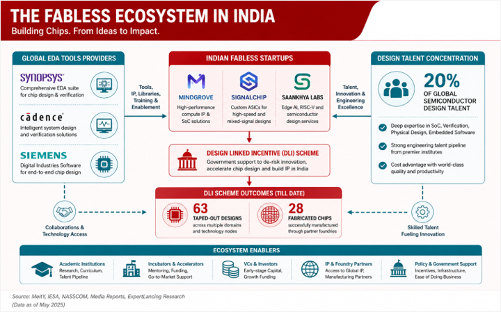
The global EDA market is dominated by three major players: Synopsys, Cadence, and Siemens EDA. These companies provide software tools for designing and verifying integrated circuits, systems-on-chips, and semiconductor intellectual property. The Design Linked Incentive scheme has catalyzed significant activity in this segment, supporting 63 taped-out designs and 28 fabricated chips through financial incentives and design infrastructure support.
The Indian government’s initiative to democratize chip design by providing Indian universities with access to industry-grade EDA tools in India represents a foundational investment in human capital. This program addresses a critical challenge: while India possesses substantial design talent, access to commercial-grade software has historically been limited for educational institutions and startups. By removing this barrier, the government is cultivating the next generation of semiconductor designers and enabling fabless startups to develop competitive products.
The fabless ecosystem in India is gaining momentum with over 50 semiconductor startups, including Mindgrove, Signalchip, and Saankhya Labs, driving innovation in artificial intelligence and automotive applications. These companies rely entirely on EDA tools for their design operations, making the software infrastructure as critical as physical manufacturing capabilities for their success. For India, the growth of EDA tools, fabless startups, and semiconductor design talent can become a major pillar of the broader semiconductor supply chain India strategy.
The Path Forward: Integration and Indigenous Capability
The transformation of India’s semiconductor ecosystem from an import-dependent structure to a self-reliant manufacturing base requires coordinated progress across materials, equipment, and EDA domains. The recent inauguration of CG Power’s G1 OSAT pilot line in Gujarat, capable of handling 0.5 million chip units daily, and the establishment of Micron’s ATMP facility represent tangible progress in manufacturing capabilities. However, the true measure of success will be the degree to which these facilities source materials and equipment from Indian suppliers.
The talent dimension remains both a strength and a constraint. While India contributes 20% of global semiconductor design talent, the industry faces a shortage of professionals with expertise in fabrication unit management and scaling. Lam Research’s commitment to train 60,000 Indian engineers through a dedicated semiconductor training lab addresses this gap, but the industry will need to generate approximately one million jobs by 2026 to meet projected demand.
Recommendations for Stakeholders
For Government Policymakers: Prioritize R&D investment in high-purity chemical production and establish technology transfer partnerships with established materials suppliers in Japan, South Korea, and Germany. The current allocation of 2.5% of the PLI outlay to R&D is insufficient for developing indigenous capabilities in critical materials and equipment components.
For Domestic Conglomerates: Evaluate opportunities in semiconductor materials manufacturing, particularly in specialty chemicals and gas supply chains where India’s existing chemical industry provides a foundation for vertical integration. The capital requirements are substantial, but the strategic value of securing supply chains is considerable.
For Global Equipment Manufacturers: Expand engineering and development operations in India beyond sales and support functions to include genuine research and development activities. The concentration of design talent and the growth of domestic manufacturing create conditions for innovation that can serve global markets.
For Educational Institutions: Deepen collaboration with industry to ensure curriculum alignment with emerging requirements in fabrication technology, materials science, and EDA tool proficiency. The government’s initiative to provide EDA tool access to universities should be complemented by faculty development programs to ensure effective utilization of these resources.
How ExpertLancing Helps Companies Map Semiconductor Supply-Chain Opportunities
As India’s semiconductor ecosystem expands, companies need clearer visibility into where opportunities are emerging across materials, equipment, EDA tools, talent, and supplier partnerships. ExpertLancing helps businesses map semiconductor supply-chain opportunities by identifying relevant market segments, potential partners, technology gaps, compliance requirements, and investment priorities. For companies entering or expanding in India’s semiconductor sector, this intelligence can support better decisions on sourcing, partnerships, localization, and long-term market positioning.
The next phase of India’s semiconductor growth will not be defined by fabs alone. It will be shaped by the strength of the supporting ecosystem: semiconductor materials, equipment, skilled talent, resilient supply chains and EDA tools in India. Companies that understand this missing layer early will be better positioned to participate in India’s semiconductor future.