Asia semiconductor investment is spreading by stage. Korea and China race for memory scale while Vietnam, India, Thailand and Japan pull testing, substrates and mature-node fabs into new places. The prize goes to whoever builds supplier depth.
In October 2026, Samsung affiliates outlined 12.26 trillion won (USD 9.15 billion) of chip spending. Nearly 8 trillion won of it is earmarked for Vietnam, not Korea. That split tells us more about Asia semiconductor investment than any single fab announcement.
Our thesis on Asia semiconductor investment is simple. Asia semiconductor investment is no longer one race for fabs. It is a redistribution of stages. Memory and wafer depth stay concentrated in Korea and China, while testing, substrates and mature-node plants move outward. The economies that build suppliers and skills, and not only plants, will keep the value.
Where Asia Semiconductor Investment Is Going
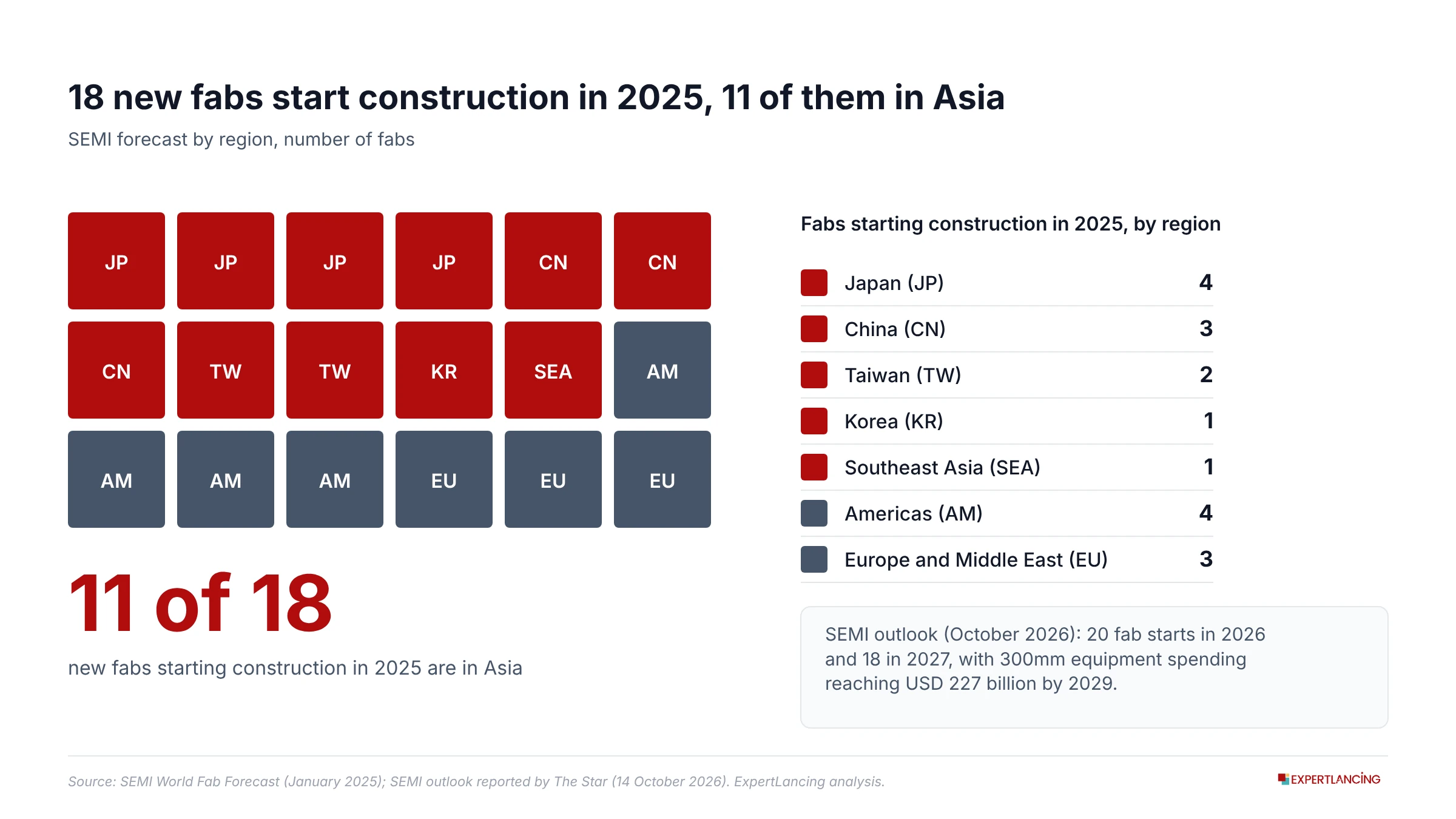
Industry data gives the best count of new capacity. SEMI expected 18 new fabs to start construction in 2025, and eleven of them sit in Asia. Japan has four, China three, Taiwan two, Korea one and Southeast Asia one. The Americas took four, and Europe with the Middle East took three.
The pace has not slowed. SEMI’s latest outlook lists 20 starts in 2026 and 18 in 2027. It also projects 300mm equipment spending of USD 149 billion in 2026, rising to USD 227 billion by 2029. Construction spending should grow 23 percent to USD 47.5 billion in 2026. It then rises 33 percent to USD 63.3 billion in 2027. Meanwhile 13 fabs start operating in 2026 and 23 in 2027.
Asia is not the only destination. Americas equipment spending is forecast to rise from USD 18.1 billion in 2026 to USD 40.6 billion in 2029. Asia semiconductor investment therefore competes with a fast-growing Western programme for tools and talent.
A fab count can mislead, though. One Korean memory fab can outweigh several mature-node plants in wafer volume. The headline number therefore shows where ground is broken, not where capacity concentrates.
Korea Scales Memory and Sends Finishing Work Abroad
South Korea anchors Asia semiconductor investment in memory, and it is building for volume at home. Samsung plans six fabs at its Yongin site, and SK hynix plans four fabs at a separate Yongin cluster. A Korean industry foundation head puts the memory supply gap at 30 to 40 percent. Earlier price swings followed imbalances of only about 2 percent.
New capacity will arrive slowly, because construction, equipment installation and qualification take years. Lines are likely to open in stages as yields improve. That is why the Vietnam plans matter for the wider chip supply chain.
Also Read: Why India’s Semiconductor Sovereignty Runs Through Mature Nodes, Not a Race to 3nm
Vietnam Takes Final Testing and Substrate Work
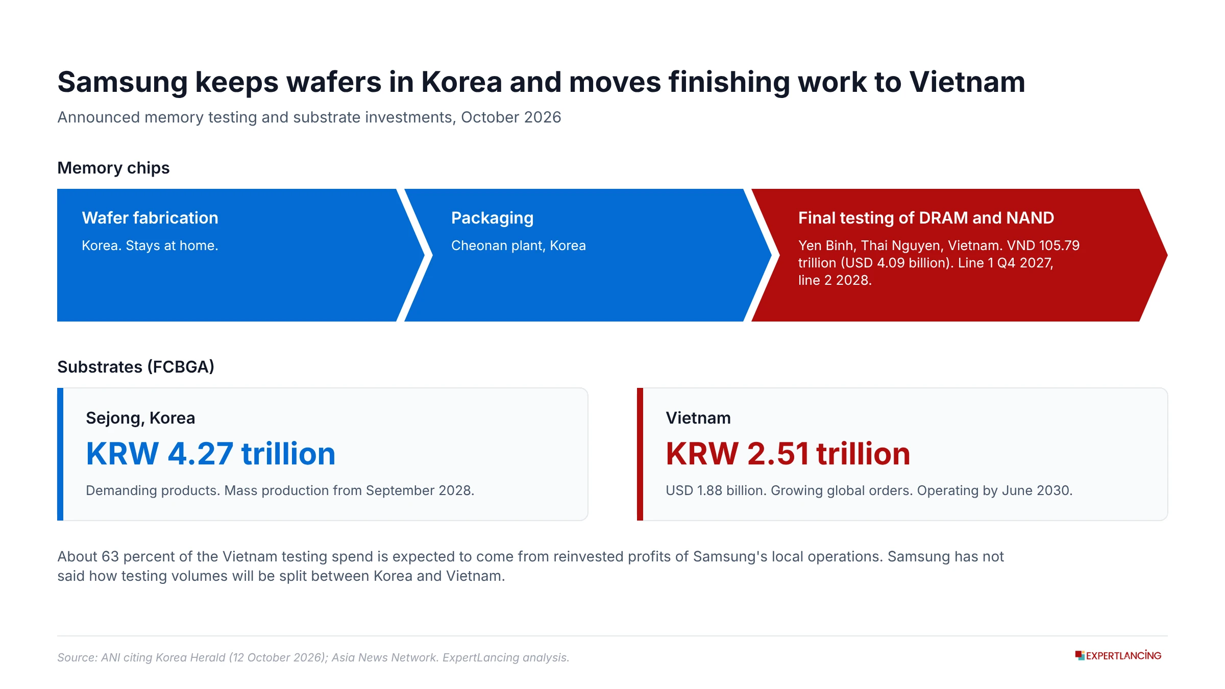
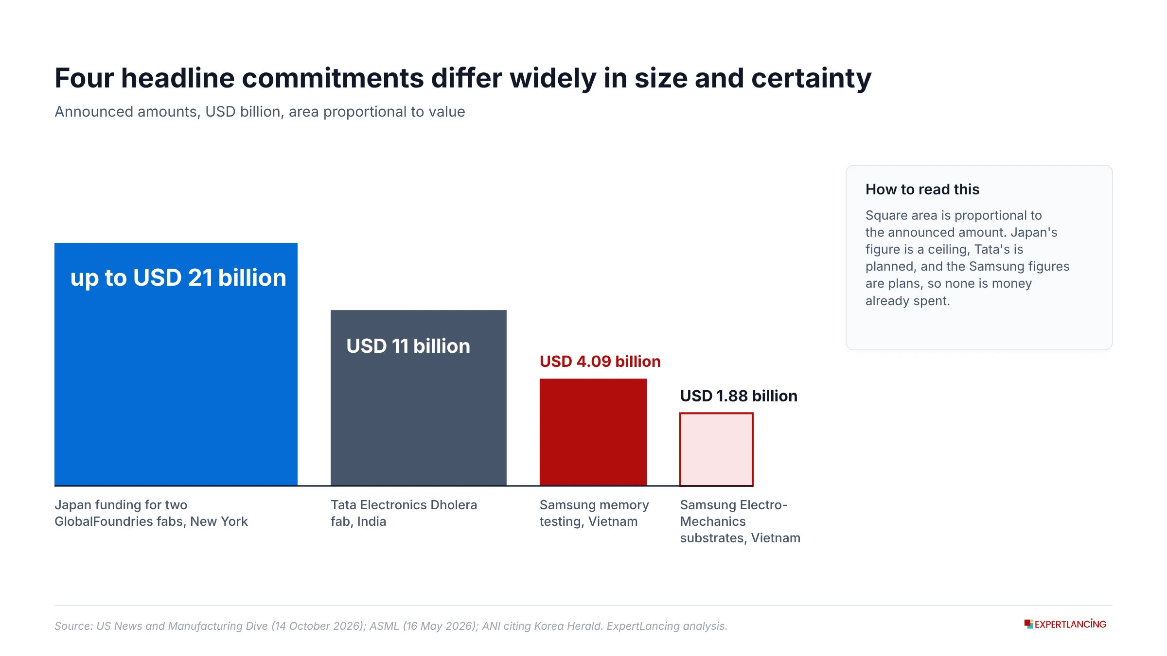
Samsung Electronics intends to spend 105.79 trillion dong (USD 4.09 billion) on memory testing at Yen Binh in Thai Nguyen. The first line is due in the fourth quarter of 2027, and a second follows in 2028. These sites will run final tests on DRAM and NAND chips packaged at the Cheonan plant in Korea. Wafers will still be made at home.
Funding is revealing as well. Samsung’s local operations are expected to supply about 63 percent from reinvested profits. The plan therefore grows on an existing Vietnamese base. One Korean academic suggests high-value products such as high-bandwidth memory may stay in Cheonan and Onyang.
Samsung Electro-Mechanics follows the same logic. Its 6.78 trillion won substrate plan puts 4.27 trillion won into Sejong, for demanding products from September 2028. The other 2.51 trillion won (USD 1.88 billion) goes to Vietnam for growing global orders by June 2030.
So Korea keeps the high-value steps and exports the volume steps, which is a new pattern for Asia semiconductor investment. Samsung has not said how testing will be split between the two countries. An industry source quoted in the coverage also warns that plants abroad do not build a local ecosystem. Both points deserve attention.
India Builds From the Back End Toward the Fab
India shows the opposite pattern in Asia semiconductor investment. It started with assembly and test, and it now wants the front end. On 16 May 2026, Tata Electronics and ASML signed a memorandum for the Dholera fab in Gujarat. The planned USD 11 billion investment would create India’s first commercial 300mm fab.
The plant targets 28, 40, 55, 90 and 110 nanometre nodes through Tata’s partnership with PSMC of Taiwan. ASML would supply its lithography tools, and the partnership also covers talent training and research infrastructure. These are mature nodes aimed at automotive, mobile and AI uses. The strategy is breadth for local demand, not a race to the leading edge.
Packaging is already under way. Kaynes Semicon began commercial operation at Sanand on 31 March 2026. The plant cost about 3,300 crore rupees. That gives India a working back end to feed from, which matters for any new fab.
Policy now targets the weakest link. The cabinet cleared Semicon 2.0 on 15 July 2026 with a USD 13.5 billion outlay and six pillars. They cover design, equipment and materials, extra fabs, advanced packaging, applied research and talent. That figure is programme support, not money already spent, so delivery will decide its worth.
Japan Funds Capacity Outside Its Own Borders
Japanese capital is also reshaping the map of Asia semiconductor investment, and some of it lands outside Asia. Japan will provide up to $21 billion for two GlobalFoundries fabs at Malta, New York. The money flows through a US and Japan trade and investment initiative.
About USD 10 billion pays for the first 300mm fab. Groundbreaking is planned later in 2026, and opening is planned for 2029. A second fab of roughly the same cost would follow at a later date. Each fab should add about 900,000 wafers of US capacity a year. More than 1,000 skilled jobs should follow.
The US side attaches conditions. The Commerce Department will redirect $955 million of an existing CHIPS award toward silicon photonics, silicon germanium and advanced packaging. It will also take a stake of about 4 percent in the company.
For readers tracking Asia semiconductor investment, the lesson is that Asian money now follows customers and policy wherever they sit. The risk is plain too, because the second fab still depends on later funding.
China Scales Output and Fences In Its Know-How
China remains the volume story in Asia semiconductor investment. Its integrated circuit output reached 484.3 billion units in 2025, up 10.9 percent on the year. That is about 4.5 times the 108.72 billion produced in 2015. The growth spans mature nodes, memory, packaging and equipment.
Beijing is also tightening control of what leaves the country. A draft export catalogue published on 16 October covers 40 technologies. It includes design know-how for AI processors at 14 nm or more advanced nodes. Chips built with 2.5D or 3D advanced packaging fall inside the same scope. An interim filing rule now applies to outbound transfers of the named technologies.
This changes how foreign partners should read Asia semiconductor investment in China. Capacity is expanding fast. Yet transfers of design and packaging knowledge may soon need licences. Partners with China-linked ventures should map that exposure early.
Also Read: Advanced Semiconductor Packaging: Winning the New Chip Race
Thailand Sets a Thirty-Year Ladder
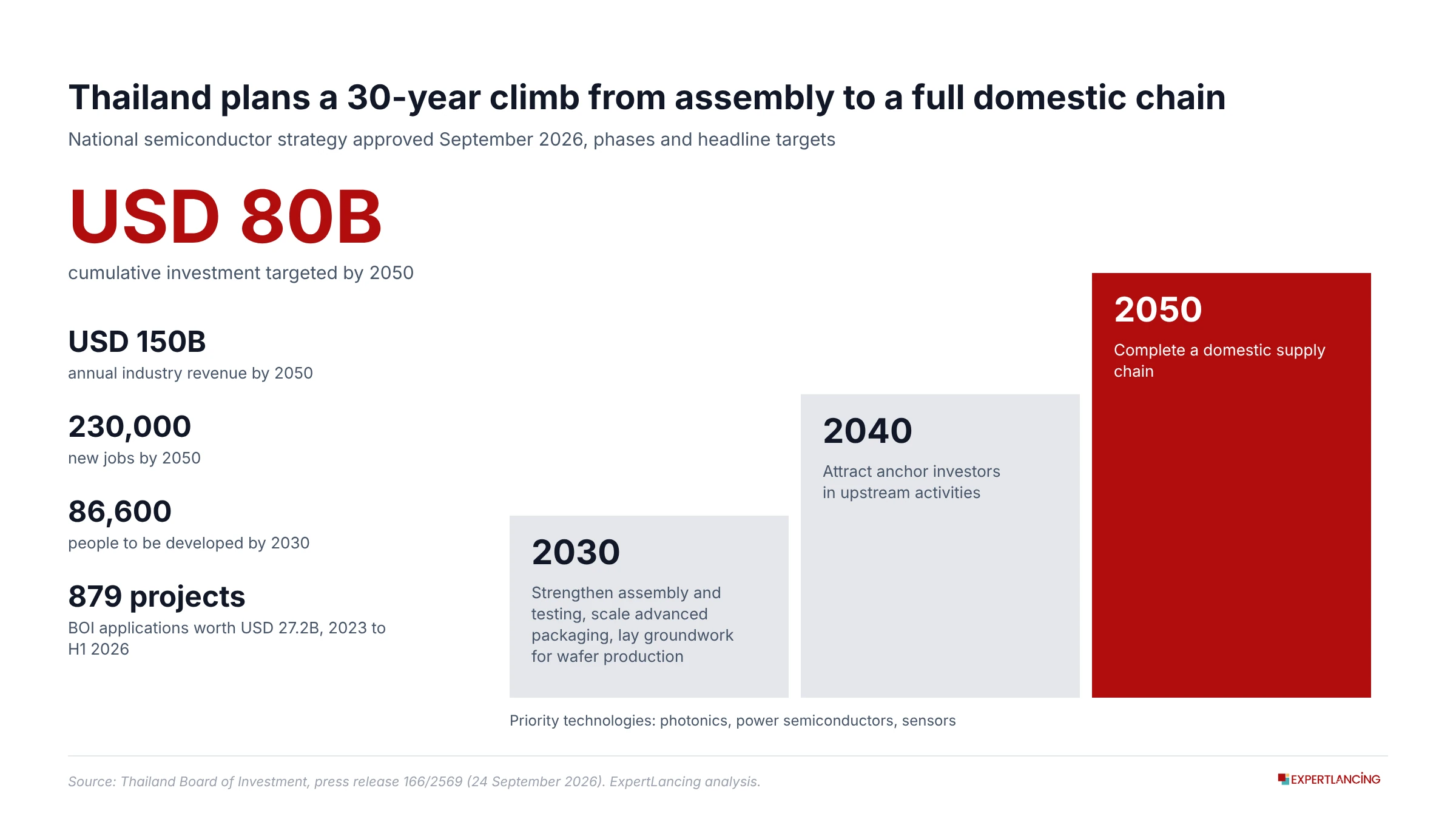
Thailand joins Asia semiconductor investment late, with a long plan. Its first national semiconductor strategy, approved in September 2026, targets about USD 80 billion of cumulative investment by 2050. It also aims for about USD 150 billion in annual revenue and more than 230,000 new jobs.
The plan moves in steps. Phase one runs to 2030: it strengthens assembly and testing, scales advanced packaging and prepares the ground for wafer production. By 2040 the plan seeks anchor investors in upstream activities. The final phase, by 2050, aims for a complete domestic supply chain. Photonics, power semiconductors and sensors are the priority technologies.
Talent is the binding constraint on Asia semiconductor investment in Thailand, so the workforce target is notable. The plan aims to develop 86,600 people by 2030, and 84,900 of them would be highly skilled. Tax incentives, grants and low-interest financing back the effort. Investor interest is already visible. Between 2023 and the first half of 2026, the investment board received 879 project applications worth about USD 27.2 billion.
What Decides Who Keeps the Value in Asia Semiconductor Investment
Read together, these programmes share one weakness, and it limits the chip supply chain they are meant to strengthen. Plants can be financed and announced within a year. Supplier networks, engineers and process know-how take a decade. Korean industry voices say so, and India has put equipment and materials into Semicon 2.0 because the gap is real.
There is a fair counterargument. Back-end capacity is a sound entry point, and the Vietnam and Thailand plans may pull suppliers in over time. That outcome is plausible but unproven. The evidence so far shows plans and not supplier clusters.
For buyers, Asia semiconductor investment looks different from the host government’s view. A purchasing head cares about qualification time, test capacity and licensing risk more than about plant announcements. On those measures, Korea and China still hold most of the depth. The newer hubs are options for the end of the decade.
Also Read: Semicon 2.0: India Semiconductor Scheme Analysis
Conclusion: Asia Semiconductor Investment Rewards Supplier Depth
Asia semiconductor investment is spreading by stage, not only by country. Korea scales memory while shifting final testing and substrates to Vietnam. India is moving from packaging toward a 300mm fab, and Japan is financing capacity abroad. China grows output while guarding design know-how, and Thailand has set a ladder to 2050.
Three facts carry the argument. They are the Samsung split between Korea and Vietnam, the Tata and ASML memorandum, and the draft Chinese export list. Over the next two quarters, watch for three signals. They are groundbreaking at Malta, a firm timetable for the Vietnamese test line, and the final scope of China’s catalogue.
Analyst’s Point of View
We think the next decade of Asia semiconductor investment will reward supplier depth more than plant count. Back-end sites seem a sensible first step. They could stay assembly outposts, however, if equipment, materials and engineering talent do not follow. The main uncertainty for Asia semiconductor investment is delivery, since several programmes remain announced intentions. Evidence of local suppliers opening plants near these sites would change our view.
Does Your Supply Chain Depend on Asian Chip Capacity?
Understanding Asia’s semiconductor landscape requires a clear view of manufacturing capabilities, supply chain dependencies, and competitive developments across the region. ExpertLancing’s Semiconductor and Industrial Practice supports manufacturers, investors, and policy teams with IP research, technology advisory, and market intelligence. Its capabilities include patent landscape analysis, technology assessments, and competitive intelligence, helping organisations assess semiconductor value chains, identify potential partners, and evaluate regional exposure to evolving industry dynamics.
With 60+ professionals in India and a global presence across the USA and Japan, ExpertLancing brings together IP researchers, technical experts, and domain specialists across multiple technology and industry domains.
Looking to assess semiconductor supply chains, evaluate potential partners, or gain deeper regional insights? Connect with our experts to discuss your requirements.
About The Author