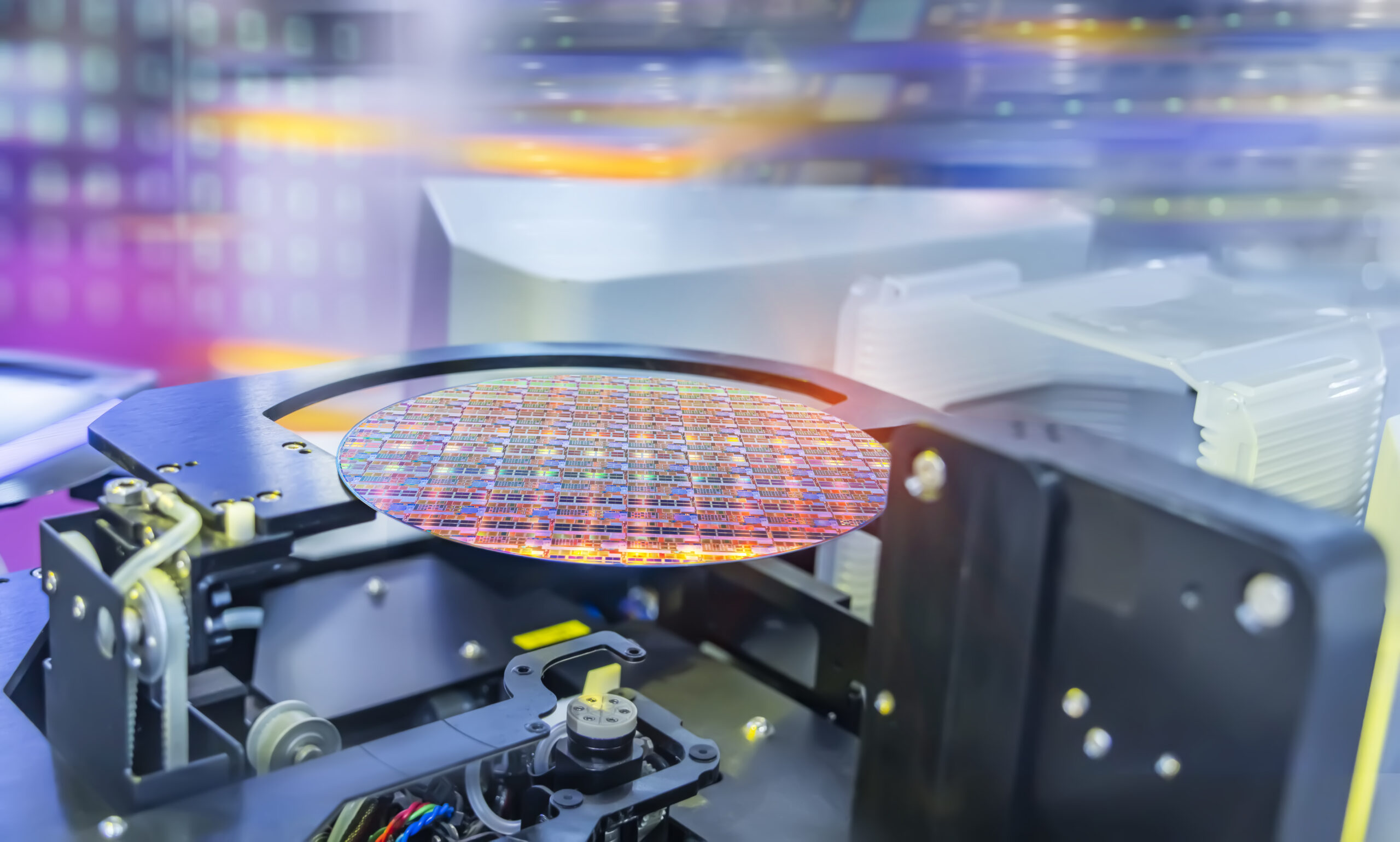
The new chip race is no longer being decided by transistor size alone. Advanced semiconductor packaging is emerging as the next competitive battleground, as AI workloads push compute, memory, bandwidth, and thermal requirements beyond what a single die can efficiently deliver. The companies that can bring these elements together through 2.5D and 3D architectures, high-bandwidth memory, chiplets, and advanced interconnects will increasingly determine where the next generation of computing performance comes from.
The Node Race Has Slowed. The Package Is Where the Fight Moved.
A chip today can have the best transistors in the world and still lose the performance race, because the bottleneck sits outside the transistor. Flip-chip packaging, the workhorse technology of the last three decades, is worth close to $27 billion and is growing at 6.3 percent a year, but the real money and the real performance gains have shifted to 2.5D and 3D IC packaging (Source: McKinsey & Company, The Growth of Advanced Semiconductor Packaging, 2023).
This segment alone is now valued between $55 billion and $68 billion in 2025 and is projected to cross $160 billion by 2035, growing faster than 11 percent a year (Source: Astute Analytica, Advanced Semiconductor Packaging Market Report, 2025). For any CXO in the semiconductor and electronics value chain, advanced packaging performance optimization is no longer a back-end manufacturing detail. It is where product differentiation now happens.
| Year | Market Size (USD Bn) |
| 2024 | 45–60 |
| 2025 | 55–68 |
| 2030 | ~95 (estimated, interpolated at 11.3% CAGR) |
| 2035 | 160 |
Source: Astute Analytica, Advanced Semiconductor Packaging Market Size, 2025.
Why Performance Optimization Has Moved Into the Package
The core engineering problem is simple to state and hard to fix. Compute engines have scaled faster than the ability to feed them data. Industry analysts call this the memory wall. Cores and AI accelerators can multiply in number, but moving data between logic and memory across long, off-package traces costs too much power and too much time.
High bandwidth memory, or HBM, solves this by sitting physically closer to the compute die, and each modern AI accelerator socket now integrates up to twelve HBM cubes delivering over 3 terabytes per second of sustained bandwidth.
My own reading of this shift is that companies are still budgeting for packaging the way they did ten years ago, as a cost center to be minimized. That thinking is now outdated.
Deloitte estimates chiplet-based solutions alone will generate $100 billion to $110 billion in revenue in 2026. This is fundamentally a packaging story, not a design story. At the same time, lead times for advanced packaging capacity, particularly TSMC’s CoWoS process used for Nvidia’s AI accelerators, remain stretched to 52-78 weeks even after near-quadrupling capacity since 2024. (Source: Deloitte, TMT Predictions 2026: Semiconductor Supply Chains, 2026; Astute Analytica, Advanced Semiconductor Packaging Market Report, 2025.).
Any company treating packaging as an afterthought in its product roadmap is planning against a capacity reality that no longer exists.
| Year | CoWoS Capacity (k wafers/month) | Reported Lead Time (weeks) |
| 2024 | ~35 | 40–50 |
| 2025 | ~90 | 45–60 |
| 2026 (target) | ~130 | 52–78 |
This is the clearest sign that advanced packaging has become a supply-constrained industry layer rather than a simple manufacturing step. Even as TSMC pushes capacity toward 130,000 wafers a month, roughly a fourfold jump since 2024, order lead times have not come down; they have stretched further, because AI accelerator demand is growing faster than capacity can be added. For any category or supply chain leader, this single chart makes the case for booking packaging slots far earlier than a typical component procurement cycle would suggest.
What Leading Companies Are Actually Doing
TSMC is pushing CoWoS wafer output toward 130,000 wafers a month and has moved to CoWoS-L at 3.5x reticle size to keep pace with silicon interposer demand from Nvidia, Google, and Amazon. Intel and Samsung are also pursuing hybrid bonding approaches including Foveros and equivalent 3D stacking platforms, that push interconnect pitches below 10 micrometers.
Standards bodies are catching up as well, with Universal Chiplet Interconnect Express, or UCIe, emerging as a common interface for integrating chiplets from different vendors and process nodes. (Sources: IDTechEx, Advanced Semiconductor Packaging 2025-2035, 2024; HCLTech, Semiconductor Trends 2026, 2026.)
What This Means For You: If you are running supply chain or category strategy for an electronics or automotive business that depends on advanced silicon, the practical takeaway is to stop treating packaging capacity as guaranteed and start treating it as allocated. Book capacity through OSAT and foundry partners eighteen months ahead of a product launch, not six, and build a second packaging source into every critical design, because the same 2.5D and 3D IC packaging plants building HBM stacks for AI accelerators are the ones your automotive and industrial chips compete for capacity with.
India is entering this story from the assembly and test side. Micron’s $2.75 billion ATMP facility in Sanand and CG Semi’s OSAT plant, inaugurated by the Prime Minister on 4 July 2026, mark India’s first commercial-scale packaging operations, alongside Kaynes Semicon’s unit targeting 6.3 million chips a day (Source: India Semiconductor Mission, ISM Programme Updates, 2026). Tata Electronics’ Assam facility is designed to reach 48 million chips a day at full scale (Source: IMARC Engineering, Semiconductor Manufacturing Expansion in India, 2026).
| Facility | Location | Investment | Design Capacity | Status (mid-2026) |
| Micron ATMP | Sanand, Gujarat | $2.75 billion | Not disclosed | Inaugurated 28 Feb 2026 |
| Kaynes Semicon OSAT | Sanand, Gujarat | ₹3,300 crore | 6.3M chips/day | Commercial, Mar 2026 |
| CG Semi OSAT | Sanand, Gujarat | ₹7,600 crore | 4.7Bn units/yr (peak) | Inaugurated 4 Jul 2026 |
| Tata Electronics ATMP | Jagiroad, Assam | ₹27,000 crore | 48M chips/day | Under construction |
Three plants inaugurated in one town within about five months is a genuine cluster forming, not a series of standalone press events. But every one of these is an assembly, test, and legacy packaging operation. None of them, as things stand today, does silicon interposer or hybrid-bond 2.5D/3D work, which is where the premium margin in advanced packaging actually sits.
The Gaps Nobody Is Talking About
The first gap is that India’s packaging build-out, however impressive in speed, sits almost entirely in traditional wire-bond, flip-chip, and legacy assembly, not in the 2.5D and 3D advanced packaging that captures the premium margin. Taiwan’s ASE Technology alone held 44.6 percent of the global OSAT market in 2024, and Chinese players such as JCET and HT-Tech grew 19 to 26 percent that year, while India currently has zero companies in the global top tier (Source: Startup Fortune, citing TrendForce OSAT Rankings, 2026). Closing that gap needs glass and silicon interposer capability, not just more assembly lines.
When the same pipe becomes the attack surface
The Jaguar Land Rover attack was not isolated. Upstream Security’s 2026 Global Automotive and Smart Mobility Cybersecurity Report, now in its eighth year, analyzed 494 publicly reported incidents in 2025 and found ransomware accounted for 44 percent of them, more than double the 2024 share. Ninety-two percent of attacks were conducted remotely, 86 percent of those with no physical proximity to the vehicle at all. Sixty-seven percent involved telematics and cloud systems, the same infrastructure category that makes overnight OTA updates possible.
| Player / Geography | Share or Growth | Note |
| ASE Technology (Taiwan) | 44.6% market share | Global OSAT leader |
| JCET (China) | 19.3% revenue growth (YoY) | Closing gap with Taiwan |
| HT-Tech, formerly Huatian (China) | 26% revenue growth (YoY) | Fastest-growing major OSAT |
| Five Chinese OSAT firms | Cracked global top 10 (2025) | Structural shift in industry share |
| India (all players combined) | No company in global top tier | Early-stage, legacy-packaging focus |
The gap this chart exposes is not one India can close by building more assembly lines faster. Taiwan and China are pulling ahead specifically in advanced, high-margin packaging technology, while India’s current strength is speed of construction in traditional ATMP and OSAT work. Unless Indian OSAT players make a deliberate move into interposer and hybrid-bonding capability, the country’s packaging story will stay a volume story, not a value story.
The second gap is talent, and it is more serious than most boardroom conversations suggest. Deloitte estimates the global semiconductor industry will need over one million additional skilled workers by 2030, with the shortage most acute in 3D packaging, power delivery, and design-process co-optimization roles (Source: Deloitte, cited in HCLTech Semiconductor Trends 2026, 2026). Substrate cost inflation, running above 8 percent in 2025 due to raw material constraints, compounds this problem by squeezing margins right when volumes are meant to scale (Source: Astute Analytica, Advanced Semiconductor Packaging Market Report, 2025).
Where This Goes From Here
Advanced packaging performance optimization will decide who wins the AI hardware cycle more than the next process node will, and companies that keep organizing their roadmaps around node shrinks alone will fall behind competitors who are co-designing chiplets, interposers, and thermal architecture from day one. India will build real volume in assembly and test over the next three years, but it will not compete in premium 2.5D and 3D packaging until it invests specifically in interposer and hybrid bonding capability, not general OSAT capacity. Companies that lock in packaging capacity and talent now, well ahead of their product launch dates, will set the pace. Those that wait for the next earnings cycle to take this seriously will be renting capacity from someone else’s roadmap.
Key Takeaways
Advanced packaging is the new competitive battleground. Product differentiation is increasingly driven by 2.5D/3D IC packaging rather than transistor scaling alone, making packaging a strategic capability instead of a manufacturing back-end.
AI demand is creating a packaging capacity bottleneck. Strong demand for HBM-enabled AI chips has stretched advanced packaging lead times despite significant capacity expansion, requiring companies to secure packaging capacity well in advance.
India is scaling semiconductor packaging but remains focused on legacy technologies. Recent ATMP and OSAT investments are strengthening manufacturing capacity, yet advanced capabilities such as silicon interposers and hybrid bonding are still absent, limiting participation in high-value packaging.
Technology and talent gaps remain major barriers. India lacks globally competitive advanced packaging players, while industry-wide shortages of skilled professionals and rising substrate costs could constrain future growth and competitiveness.
Success will depend on early investment and ecosystem readiness. Companies that secure advanced packaging capacity, develop specialized talent, and integrate packaging into product strategy will be better positioned to capitalize on the next wave of AI and semiconductor growth.