
Semicon 2.0 aims to build a self-reliant and globally competitive semiconductor chip design and manufacturing ecosystem in India. The Ministry of Electronics and Information Technology notification dated 31 August 2026 extends fiscal support across six pillars and ten categories, covering semiconductor design, machines and materials, fabs, ATMP/OSAT, R&D and talent development.
The scheme is broad in scope. It supports domestic semiconductor IP and chip design, provides incentives for manufacturing inputs and equipment, and sets substantial capital and revenue thresholds for wafer fabs and display facilities. It also supports advanced packaging, semiconductor R&D and workforce training.
For businesses, the main issue is fit. Different categories target very different applicants, from Indian startups and MSMEs seeking design support to large companies proposing wafer fabs or display plants. Eligibility, licensed technology, capital investment, revenue, installed capacity and ownership requirements will determine which route is relevant. Understanding these requirements is therefore critical for companies evaluating Semicon 2.0.
What Does Semicon 2.0 Cover?
The scheme divides eligible activities into six pillars and ten categories.
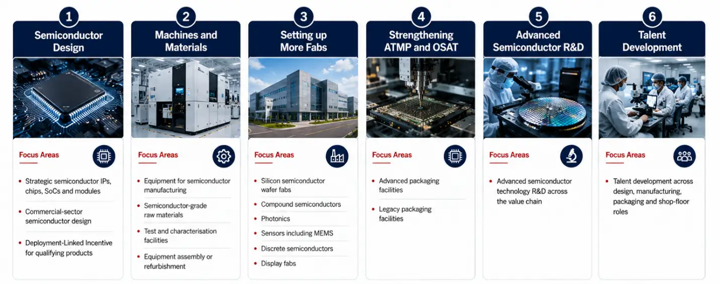
- Pillar 1 covers semiconductor design through three categories: strategic semiconductor IPs, chips, SoCs and modules; commercial-sector semiconductor design; and a Deployment-Linked Incentive for qualifying products.
- Pillar 2 addresses the manufacturing base through equipment, semiconductor-grade raw materials, test and characterisation facilities, and equipment assembly or refurbishment.
- Pillar 3 focuses on new fabs. It includes silicon semiconductor wafer fabs, compound semiconductors, photonics, sensors including MEMS, discrete semiconductors and display fabs.
- Pillar 4 covers ATMP/OSAT facilities, including advanced and legacy packaging.
- Pillar 5 supports advanced semiconductor technology R&D. Pillar 6 focuses on talent development across design, manufacturing, packaging and shop-floor roles.
This breadth matters because semiconductor competitiveness depends on more than wafer fabrication. Design capability, equipment, materials, packaging, R&D and skilled manpower all form part of the investment decision.
Semicon 2.0 for Semiconductor Design Companies
The design pillar is particularly relevant to domestic fabless companies. Category 2 aims to strengthen India as a competitive hub for semiconductor IP, chips and SoCs used in commercial electronics. Under Semicon 2.0, eligible companies can access design infrastructure and financial support depending on their project and product requirements.
Eligible companies must be incorporated and headquartered in India, maintain significant operations and manpower in the country, and be owned and controlled by Indian citizens or Overseas Citizens of India. Companies can participate independently or through consortia with global companies, R&D organisations and academic institutions.
Design Infrastructure Support includes centralised access to national EDA tools, Multi-project Wafer fabrication services, IP cores, compute sub-systems and post-silicon validation services.
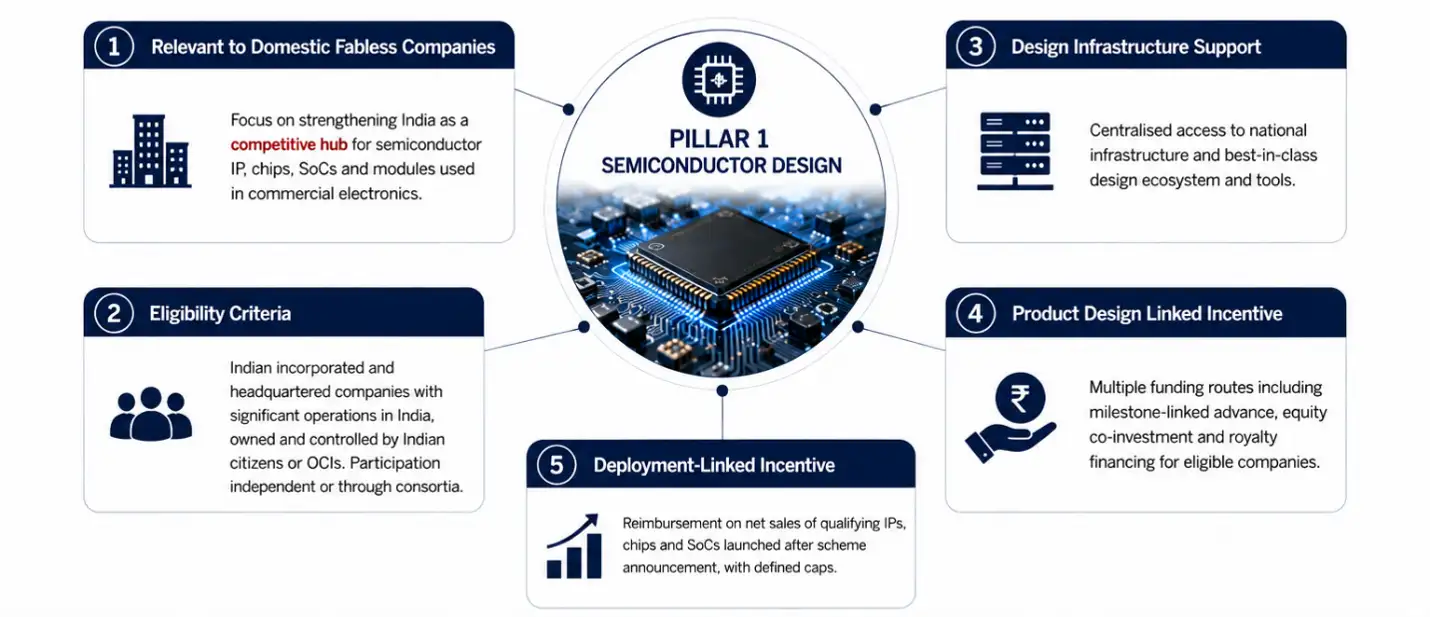
The Product Design Linked Incentive adds several funding routes. Eligible startups and MSMEs can receive milestone-linked advance seed funding equal to 50% of project cost or ₹15 crore, whichever is lower.
Equity co-investment is available beyond ₹15 crore where a company has secured funding from Venture Capital or Private Equity investors. Other eligible companies can access royalty financing, subject to the scheme conditions. Under this route, the beneficiary pays 5% of net revenue from the product or technology until an amount equivalent to 1.5 times the financial support has been recovered.
Category 3 adds a Deployment-Linked Incentive. Qualifying semiconductor IPs, chips and SoCs launched for the first time after the scheme announcement, with no prior sales by the applicant before the announcement, can receive reimbursement at 9% of net sales for five years.
The incentive is capped at ₹30 crore per application and ₹120 crore per company, including group companies, across multiple qualifying products.
Semicon 2.0 for Semiconductor Manufacturing Inputs
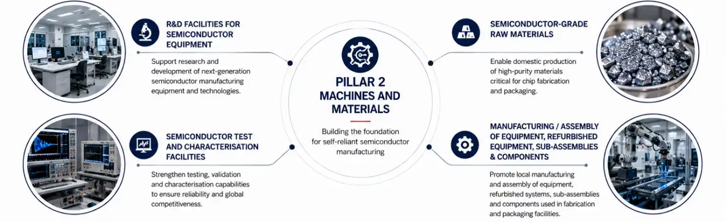
Category 4 targets the upstream manufacturing base.
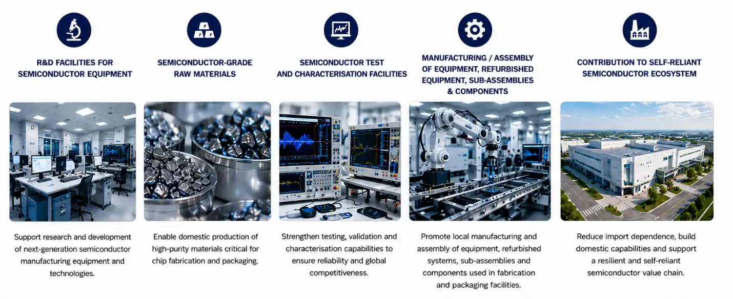
Eligible activities include R&D facilities for semiconductor equipment, semiconductor-grade raw materials, semiconductor test and characterisation facilities, and manufacturing or assembly of equipment, refurbished equipment, sub-assemblies and components used in fabrication and packaging facilities.
Applicants must generally own or possess own or possess licensed technologies for the proposed unit, except for test and characterisation facilities.
Minimum capital investment thresholds range from ₹50 crore for semiconductor-grade raw materials to ₹300 crore for semiconductor equipment R&D and equipment manufacturing or assembly. Revenue thresholds range from ₹20 crore to ₹120 crore, depending on the sub-vertical.
The government will provide support equal to 30% of eligible capital expenditure on a pari-passu basis for the relevant activities.
Equipment manufacturing or assembly also qualifies for a Production Linked Incentive of 10% / 8% / 6% / 4% / 2% of the Bill of Materials value sourced from domestic manufacturers. The PLI applies for five years starting from FY 2028-29 and is subject to an overall ceiling of 50% of eligible capex.
Large Fab Projects Face High Entry Thresholds
Category 5 is aimed at silicon semiconductor wafer fabs using 300 mm technology with installed capacity of 40,000 wafer starts per month or more.
Applicants must own or possess production-grade licensed technology for the proposed process. The minimum capital investment is ₹20,000 crore, while the minimum revenue threshold is ₹7,500 crore in any of the three financial years preceding the application year, including group companies or a joint venture.
Government fiscal support is 40% of eligible capital expenditure on a pari-passu basis.
Category 6 covers compound semiconductors, photonics, sensors including MEMS, and discrete semiconductor fabs.
The minimum capital investment is ₹500 crore and the minimum revenue threshold is ₹200 crore. Capacity and wafer-size requirements vary by technology:
- Sensor fabs require 200 mm or more.
- Compound semiconductor and discrete fabs require 150 mm or more.
- Photonics fabs require 100 mm or more.
- Capacity must be at least 500 wafer starts per month.
Fiscal support is 35% of eligible capital expenditure on a pari-passu basis.
Display Fabs and Advanced Packaging Expand the Manufacturing Scope
Category 7 covers OLED, Micro LED and LCD display fabs.
OLED projects must use Generation 6 or above technology and have capacity of at least 30,000 panels per month. The minimum capital investment is ₹10,000 crore and the minimum revenue threshold is ₹5,000 crore.
Micro LED projects require panel area of at least 500 square metres per month, ₹1,500 crore of minimum capital investment and ₹600 crore of minimum revenue.
LCD projects require Generation 8 or above technology, capacity of at least 60,000 panels per month, ₹10,000 crore of capital investment and ₹5,000 crore of revenue.
Each of these categories receives 35% support on eligible capex on a pari-passu basis.
Category 8 supports ATMP/OSAT facilities. Advanced packaging and advanced substrate projects, including 2.5D/3D packaging, wafer-level chip-scale packaging and heterogeneous integration, require minimum capital investment of ₹1,000 crore and minimum revenue of ₹200 crore.
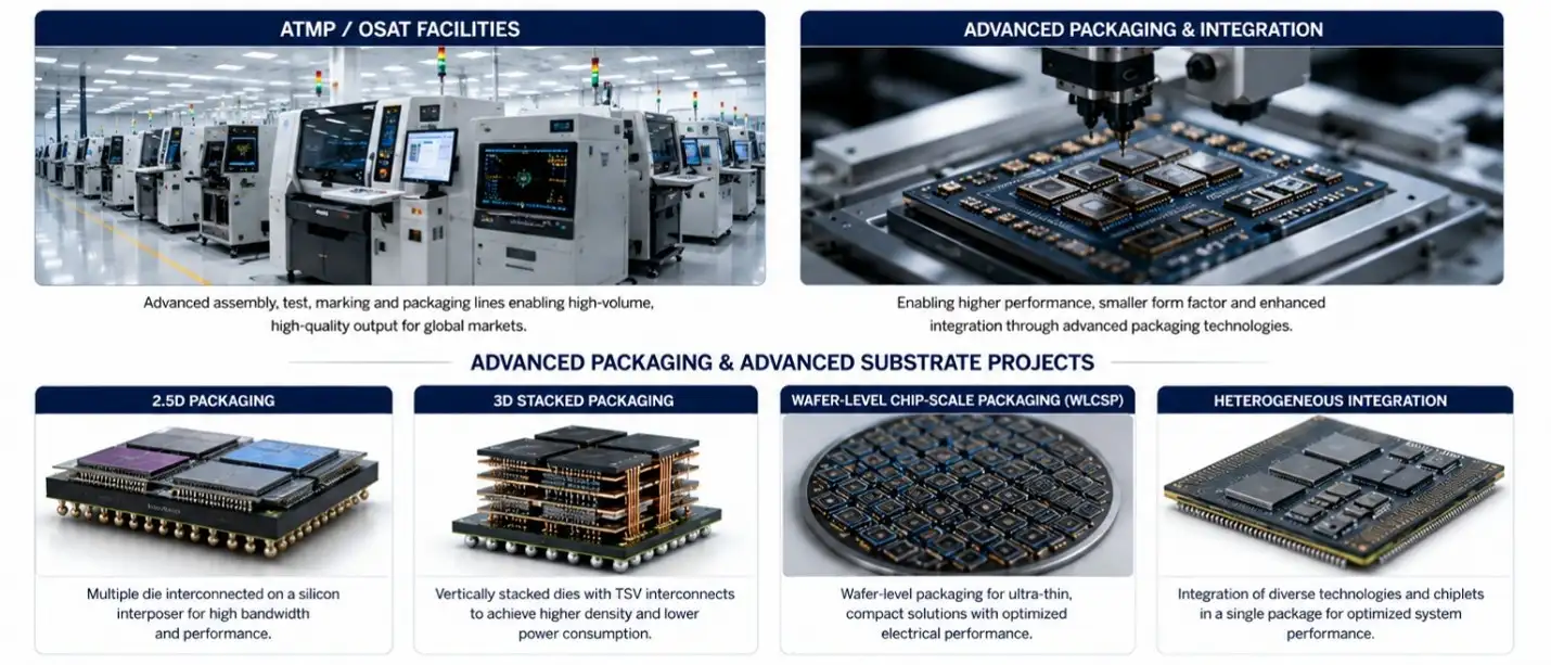
The fiscal support is 35% of eligible capex on a pari-passu basis. Legacy packaging has the same minimum capital and revenue thresholds but receives 25% support.
R&D and Talent Development Are Separate Pillars
Category 9 provides support for advanced semiconductor technology R&D.
Target areas include advanced CMOS process technologies, Silicon Photonics, display fabrication and chiplet-based technologies for advanced packaging, along with other advanced semiconductor technologies.
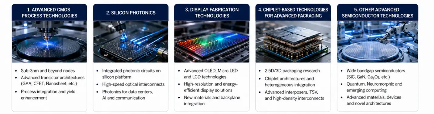
Semiconductor companies can apply independently or with academic institutions and R&D organisations.
Fiscal support can reach up to 75% of project cost, including eligible capex and opex and including State Incentive. Companies may also include RDI Scheme funding where necessary.
The Ministry will issue separate guidelines after receiving approval from the Minister for Electronics and Information Technology.
Category 10 addresses talent development.
It covers access to advanced chip design tools, MPW fabrication services and post-silicon validation tools. It also supports dedicated training infrastructure for shop-floor manpower and stronger national nanofabrication and process laboratories.
Eligible applicants include Indian academic institutions, R&D organisations and laboratories, scientific societies, and domestic training institutions or organisations.
Fiscal support can reach up to 75% of project cost, including eligible capex and opex. Project duration will be decided case by case, preferably up to six years.
How Will Applications Be Evaluated?
India Semiconductor Mission (ISM) is the nodal agency for Semicon 2.0.
ISM will invite applications, conduct technical and financial appraisal, recommend applicants and perform other responsibilities assigned by MeitY. For the three design and deployment categories, ISM may work with C-DAC.
Evaluation will consider technical and financial parameters such as process technologies, project implementation capacity, operating capability and offtake.
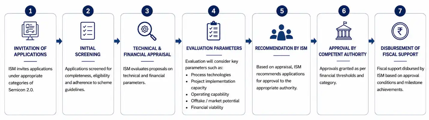
For semiconductor design categories and talent-development projects, proposals below ₹100 crore can be approved by the Secretary, MeitY.
Projects above ₹100 crore and up to ₹500 crore require approval from the Minister for Electronics and Information Technology. Projects above ₹500 crore are to be placed before the Cabinet.
Other categories are also subject to Cabinet approval after recommendation by the nodal agency.
The scheme is initially open for applications for three years. The nodal agency will disburse fiscal support based on approval conditions.
What Should Companies Assess Before Applying?
The first step is category fit. A company should map its proposed product, technology or facility against the relevant target segment before building the application. Ownership, headquarters, operational presence, revenue, capital expenditure, capacity and licensed-technology requirements can materially narrow eligibility. Companies considering Semicon 2.0 should therefore assess these requirements carefully before selecting a category and preparing an application.
The second step is the funding structure. Design applicants should compare seed funding, equity co-investment and royalty financing, including the applicable exit conditions. Manufacturing projects should incorporate the relevant capex support and, where applicable, the equipment PLI.
The third step is execution readiness. The scheme places weight on technology, implementation capacity, operating capability and offtake. A credible application will need more than a capital plan. Applicants should demonstrate that their proposed technology, project team, operating model and commercial demand align with the scheme conditions.
Conclusion
Semicon 2.0 provides a broad policy framework for semiconductor design, manufacturing, packaging, R&D and talent development in India.
Its design support is relevant to startups, MSMEs and domestic chip companies, while its fab and display categories target much larger capital-intensive projects. The upstream manufacturing categories also address equipment, materials and testing.
For companies considering an application, the immediate priority is to test category fit, quantify the funding requirement and document technology, execution and offtake readiness.
Separate scheme guidelines will also matter for categories where the notification states that further details are to be issued. The policy opportunity is substantial, but successful participation will depend on matching the project to the correct category and meeting the detailed eligibility and funding conditions.