India semiconductor ambitions face their first real test: the country’s first commercial fab will open mostly on 90nm, not 28nm. We read that as a strength. The fastest route to chip sovereignty runs through mature nodes, packaging scale and Indian-owned chip IP, not a race to 3nm that no Indian budget can fund.
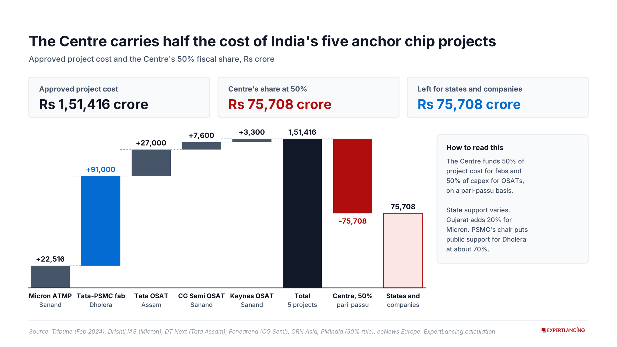
In February 2024, the Union Cabinet approved India’s first commercial fab: a Rs 91,000 crore partnership between Tata Electronics and Taiwan’s Powerchip Semiconductor Manufacturing Corporation (PSMC) in Dholera, Gujarat, sized for 50,000 wafer starts a month. The Centre funds 50% of project cost on a pari-passu basis, and PSMC chairman Frank Huang has said support from the Centre and Gujarat will cover about 70% of the outlay.
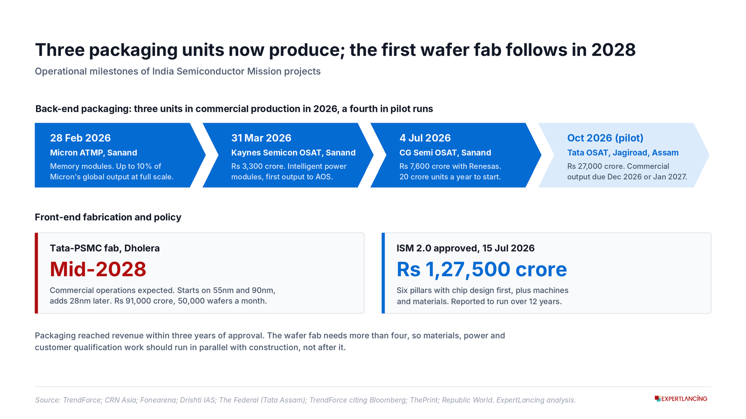
Two and a half years on, the plan has met reality. In July 2026, Bloomberg reported that Dholera will begin production mostly on 90nm. Tata Electronics says the fab will span 28nm to 110nm and that it always planned to start at 55nm and 90nm before adding 28nm. Union Minister Ashwini Vaishnaw now expects commercial operations in mid-2028, against Tata’s earlier target of end-2026.
Commentators have framed this as a setback. We disagree. Mature nodes are older process generations, typically 28nm and above, that chipmakers can produce with deep ultraviolet (DUV) lithography instead of extreme ultraviolet (EUV) tools. A node choice that keeps Dholera solvent, filled and learning serves India better than a prestige node it cannot keep busy. Restraint should become doctrine: India will earn semiconductor sovereignty through mature nodes, packaging scale and domestic chip IP, not through a race to 3nm.
Why Can’t India Compete at 3nm or 2nm?
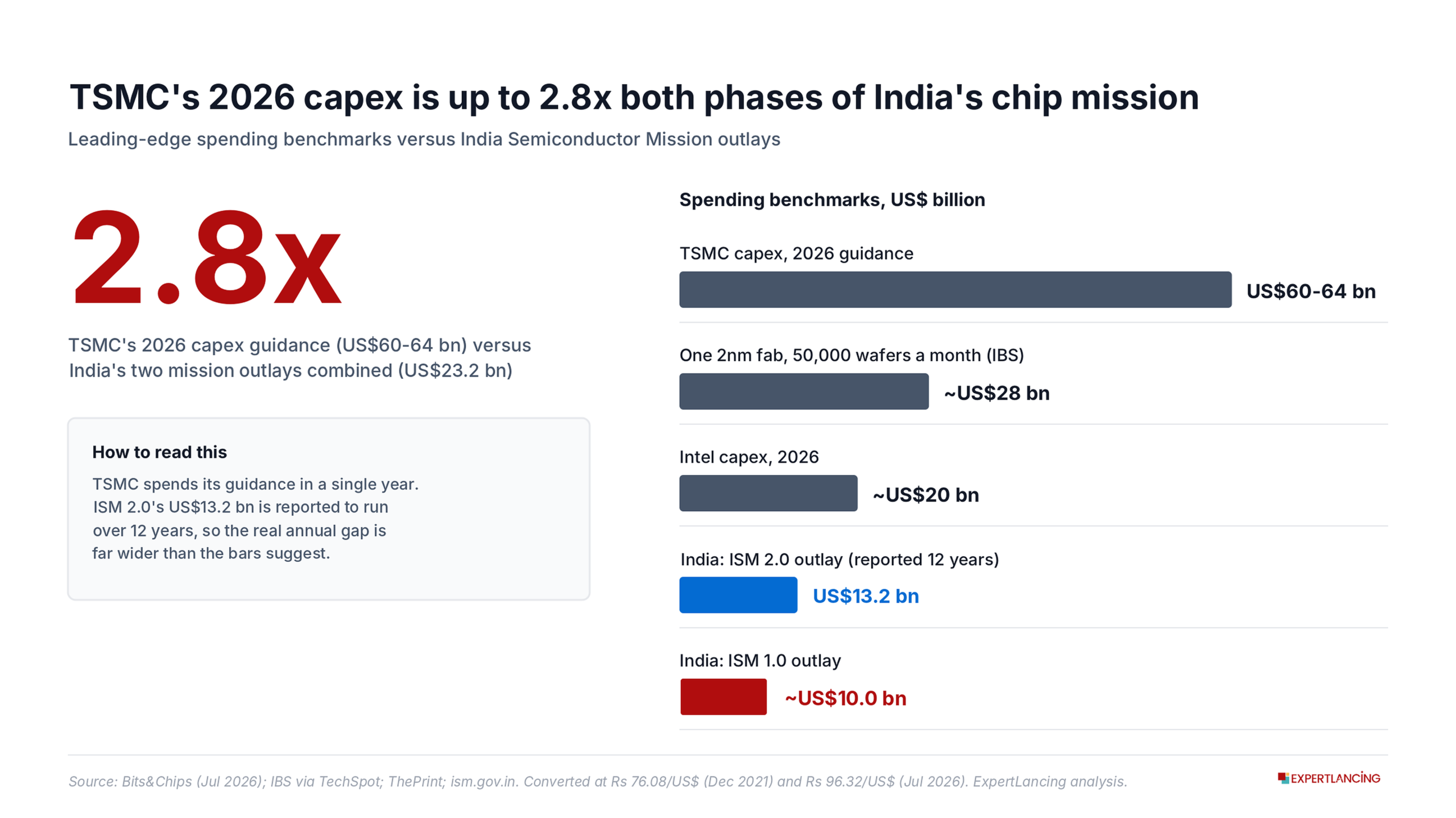
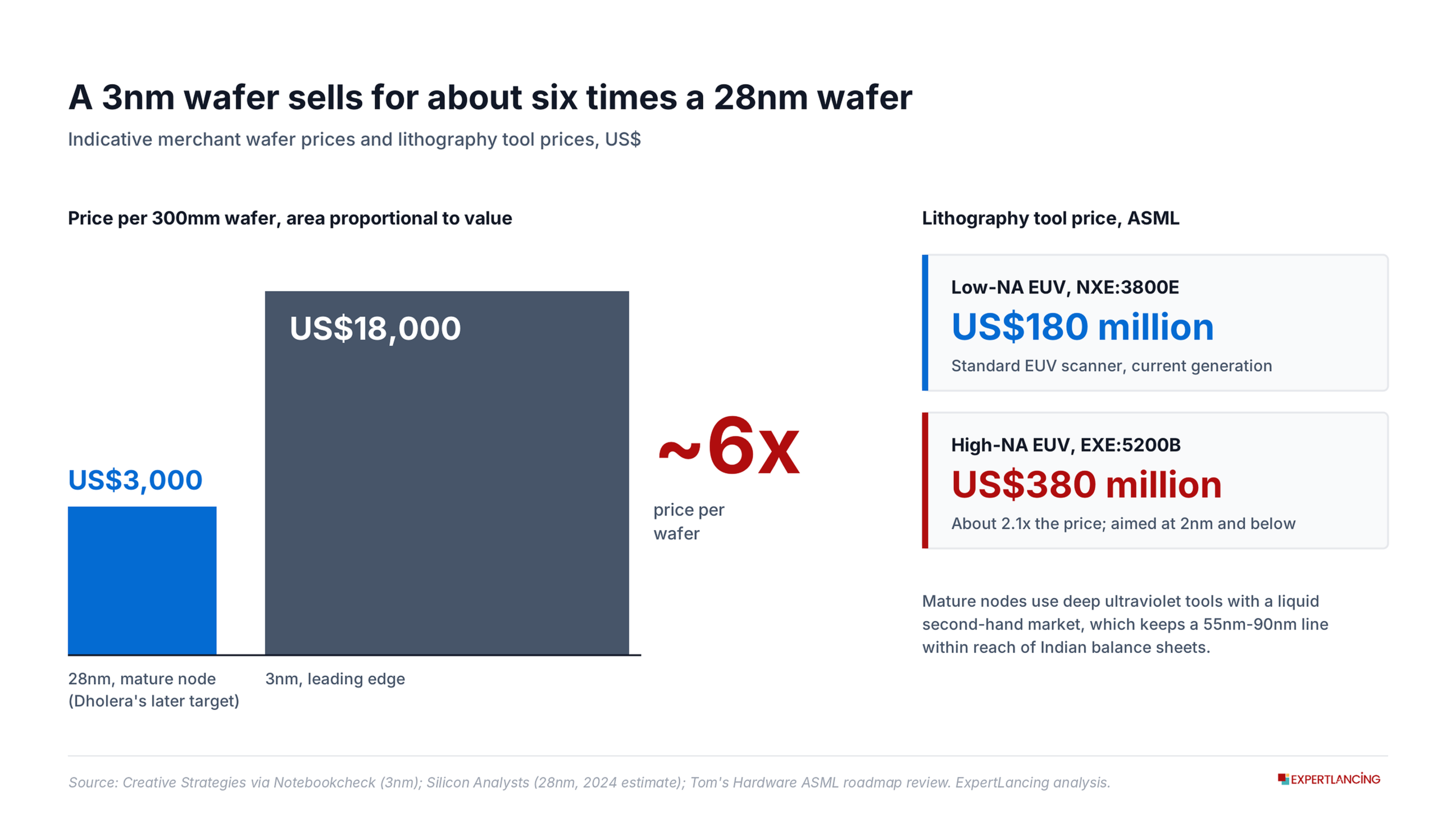
The arithmetic of leading-edge logic rules India out. Consulting firm IBS estimates that a 2nm fab with 50,000 wafer starts a month costs about US$28 billion. ASML’s High-NA EUV scanner, the EXE:5200B, costs about US$380 million per tool, roughly double the US$180 million of a standard low-NA EUV system, the NXE:3800E.
Incumbents keep raising the bar. In July 2026, TSMC lifted its 2026 capex guidance to US$60-64 billion, with 70-80% going to advanced process technology, while Intel raised its 2026 capex to about US$20 billion. Against this, India’s first mission carried a Rs 76,000 crore outlay. ISM 2.0, which the Union Cabinet cleared on 15 July 2026, adds Rs 1,27,500 crore across six pillars and runs over a 12-year lifecycle. Converted at the rupee’s rate on each approval date, Rs 76.08 to the US dollar in December 2021 and Rs 96.32 in July 2026, the two phases together come to about US$23.2 billion. One year of TSMC’s spending is up to 2.8 times both phases combined.
Wafer economics widen the gap. Creative Strategies estimates a finished 3nm wafer at around US$18,000, and other published estimates run as high as US$27,000, while industry pricing roundups put a 28nm wafer at about US$3,000. Both are analyst estimates, and contract prices vary with customer and volume. Leading-edge buyers such as Apple and Nvidia already hold deep yield-learning ties with TSMC. An Indian sub-5nm fab would depend on imported tools, imported materials and foreign customers, which is the opposite of sovereignty.
Where Does India Semiconductor Demand Sit?
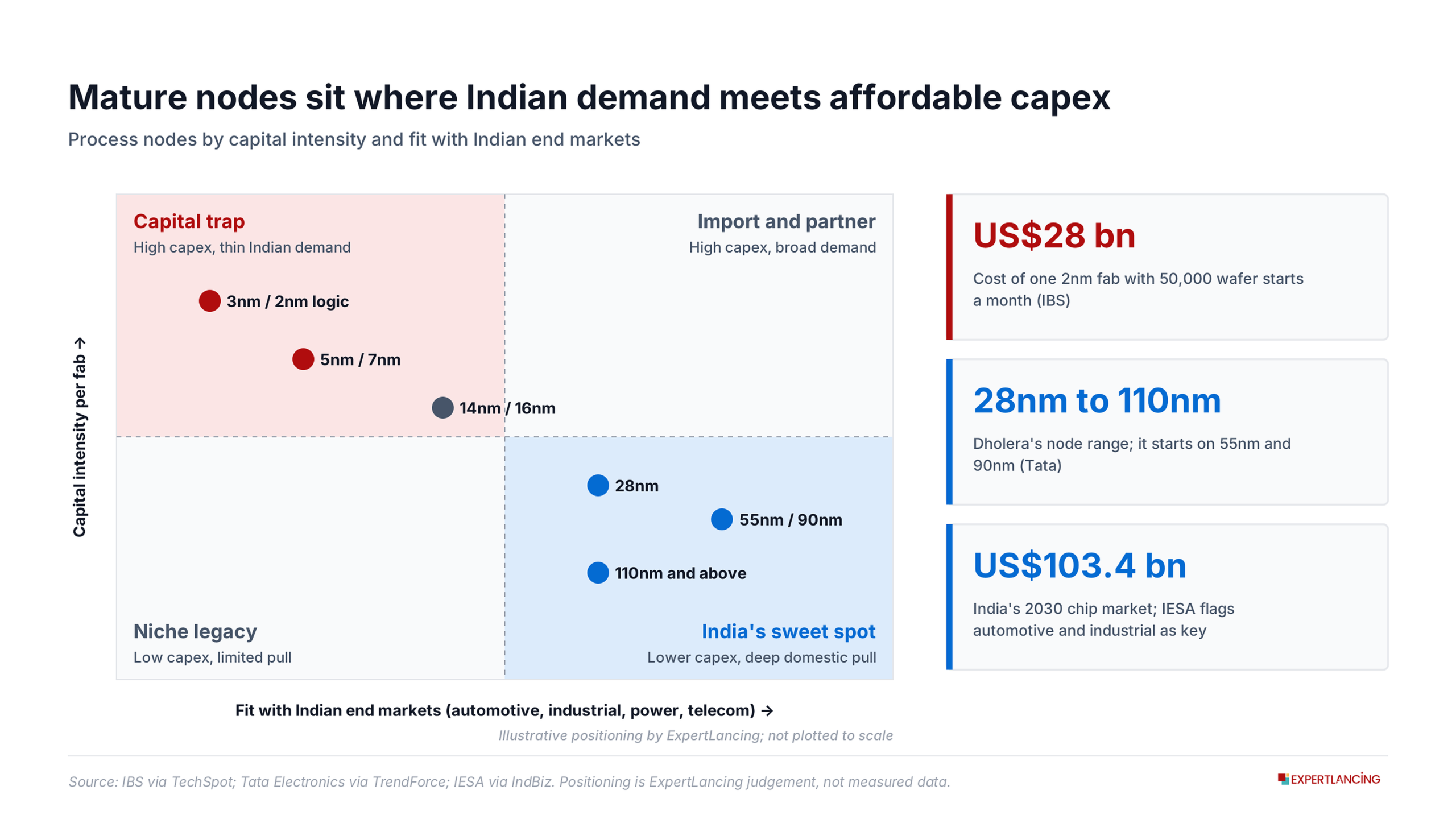
Fab strategy should follow the order book. The India Electronics and Semiconductor Association (IESA) values the India semiconductor market at US$52 billion in 2024-25 and projects US$103.4 billion by 2030, growing at 13% a year. IESA singles out automotive and industrial electronics as the main value-addition opportunities. An earlier IESA and Counterpoint Research study put the 2023 market at US$45 billion, with mobile handsets, IT and telecom contributing more than 75% of revenue.
Much of the new public infrastructure runs on mature silicon. Under the Revamped Distribution Sector Scheme (RDSS), India has sanctioned 19.79 crore consumer smart meters, and the country had installed 7.24 crore smart meters across all schemes by 30 June 2026. Each meter carries metering, communication and power-management chips that mature nodes produce well. Electric two-wheelers, rail traction, telecom and industrial automation draw on the same base.
A Dholera line that opens on 55nm and 90nm and adds 28nm later matches that demand. These nodes use DUV lithography with a liquid secondary tool market, and they serve the power, control and connectivity chips that Indian original equipment manufacturers (OEMs) buy every day.
Why Is Packaging India’s Strongest Link?
Front-end fabs take years to qualify, but India’s back-end units, which assemble, test and package chips (ATMP, or OSAT for outsourced semiconductor assembly and test), have moved from Cabinet approval to commercial output in under three years. Three units reached commercial production in 2026, and a fourth is in pilot runs:
- Micron, Sanand. The ATMP facility opened on 28 February 2026. Micron invests up to US$825 million of the US$2.75 billion total, and at full capacity the plant could supply up to 10% of Micron’s global output.
- Kaynes Semicon, Sanand. The Rs 3,300 crore unit announced commercial production on 31 March 2026. It opened with intelligent power modules for automotive and industrial use, with initial output going to Alpha and Omega Semiconductor.
- CG Semi, Sanand. Prime Minister Narendra Modi inaugurated the Rs 7,600 crore OSAT, built with Renesas and Stars Microelectronics, on 4 July 2026, marking the start of commercial production. It has capacity of 20 crore units a year and a target of 500 crore.
- Tata Semiconductor Assembly and Test, Assam. The Rs 27,000 crore Jagiroad unit is designed for 48 million chips a day using wire-bond, flip-chip and integrated system-in-package technology. It began pilot production in October 2026, and the Assam government expects commercial production in December 2026 or January 2027.
Packaging is no longer a low-margin service. As chiplets and heterogeneous integration spread, the package decides performance as much as the die. Micron’s Sanand plant is built to turn wafers from its global network into finished memory products for customers worldwide. That flow builds the quality systems, supplier base and workforce that a front-end fab will need.
Does India Own the Chips It Designs?
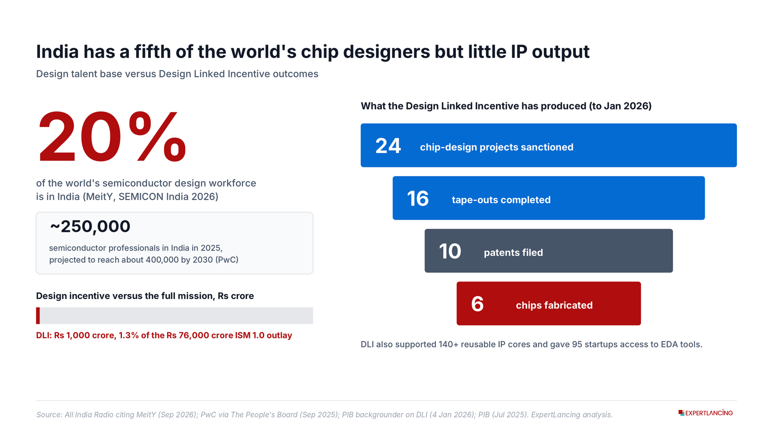
India accounts for nearly 20% of the world’s semiconductor design workforce, MeitY Secretary S Krishnan said at SEMICON India 2026 in September. Much of that talent works in the India design centres of global chip firms, so a large share of the resulting patents and royalties sits with parent companies abroad.
The Design Linked Incentive (DLI) scheme was meant to change this, but its scale is small. It carries a Rs 1,000 crore outlay, about 1.3% of the original Rs 76,000 crore mission, and caps product design support at Rs 15 crore per application. By January 2026, its 24 sanctioned projects had produced 16 tape-outs, six fabricated chips and ten patent filings. The results are real but modest for a country with India’s design depth.
ISM 2.0 makes chip design its first pillar and adds machines and materials as a pillar of its own. That is the right shift. The test now is whether funding reaches fabless firms that own their register-transfer level (RTL) designs, architecture and patents, and that design chips for Indian grids, vehicles and satellites.
What Could Stall India’s Fabs Besides Node Choice?
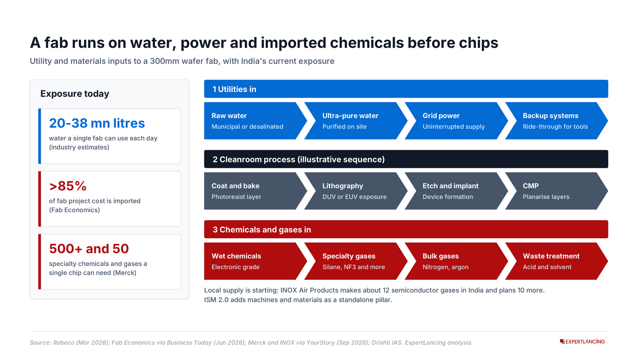
A fab is a utility customer before it is a chip maker. Industry estimates compiled by Robeco put a single fab’s water use at 20-38 million litres a day, much of it purified to ultra-pure grade. Industrial corridors must deliver that water, and uninterrupted power, before the first tool is switched on.
Materials pose a deeper risk. Fab Economics estimates that imports account for more than 85% of fab project costs and about half of wafer manufacturing costs in India today, falling to roughly 68% and 30% by 2030. Local supply is starting: INOX Air Products already makes about 12 semiconductor gases in India and plans to add 10 more. ISM 2.0’s machines and materials pillar should push this from a handful of gases to certified, multi-source supply for every critical chemical.
What Should ISM 2.0 Do Next? Three Moves
Pay for Output, Not Only for Tools
Phase one paid largely against capital spending. For ISM 2.0, MeitY and the India Semiconductor Mission should tie a growing share of fab and OSAT support to yield, utilisation and shipped volume. This protects public money from idle cleanrooms. Global technology partners will push back, so the shift should apply to new approvals and phase in over the programme’s 12 years.
Create Anchor Demand for Domestic Mature-Node Chips
A 50,000-wafer fab needs steady customers. The Ministry of Heavy Industries, the Ministry of Power and large OEMs should design advance purchase commitments for qualified domestic chips in smart meters, electric vehicles and industrial drives. Automotive qualification such as AEC-Q100 takes time, so buyers and the fab should start qualification work now, ahead of mid-2028 commercial output.
Scale the Design Incentive to Match India’s Talent
India should raise DLI funding several-fold, lift per-project caps for chips moving to volume production, and let venture-backed startups qualify as long as the core patents stay with Indian entities. High failure rates are normal in fabless startups, so rigorous technical review panels must sit alongside the money.
What to Watch Over the Next 24 Months
- First silicon and yield ramp at Dholera on 55nm and 90nm, and the timing of 28nm qualification.
- Ramp-up at Micron, Kaynes and CG Semi, and the move from pilot to commercial output at Tata’s Assam unit.
- Private Series A and B rounds for Indian fabless firms, and commercial tape-outs on mature nodes.
- Investment in electronic-grade chemicals and gases near Dholera and Sanand under ISM 2.0.
Our View: Sovereignty Is Measured in Cash Flow, Not Nanometres
India’s semiconductor programme has already delivered what many doubted: three packaging units in commercial production within a single year, a fourth in pilot runs, a funded second phase, and a fab under construction. The debate over 90nm versus 28nm misses the point. Nanometres do not define sovereignty; operating cash flow, full utilisation, local materials and owned IP do.
Our view at ExpertLancing is clear. India should treat Dholera’s mature-node start as the foundation of a profitable fab business, use packaging scale to pull materials suppliers into Gujarat and Assam, and spend far more of ISM 2.0 on Indian-owned chip design. A country with one in five of the world’s chip designers should own far more of the value it creates.
The Strategic Takeaways: From the ExpertLens
- Tata Electronics and PSMC will start the Dholera fab on 55nm and 90nm. They will add 28nm later. They now expect commercial operations in mid-2028 rather than end-2026.
- One 2nm fab costs about US$28 billion. TSMC plans US$60-64 billion of capex in 2026 alone. That is up to 2.8 times both phases of India’s chip mission combined.
- Micron, Kaynes Semicon and CG Semi began commercial chip packaging in Sanand. They did so between February and July 2026. Tata’s Assam unit entered pilot production in October 2026.
- India has nearly 20% of the world’s chip design workforce. Yet the Rs 1,000 crore Design Linked Incentive scheme has produced 16 tape-outs, six fabricated chips and ten patent filings.
- ISM 2.0 should pay for output and create anchor demand for domestic mature-node chips. It should also scale design funding to match India’s talent.
Frequently Asked Questions (FAQs)
What Process Node Will India’s First Chip Fab Use?
The Tata Electronics and PSMC fab in Dholera, Gujarat, will start mainly on 90nm and 55nm, with 28nm to follow. Tata says the fab will cover nodes from 28nm to 110nm.
When Will the Dholera Fab Start Commercial Production?
Union Minister Ashwini Vaishnaw expects commercial operations in mid-2028. Tata had earlier targeted the end of 2026.
Which Chip Packaging Plants Are Operating in India?
Micron (Sanand, February 2026), Kaynes Semicon (Sanand, March 2026) and CG Semi (Sanand, July 2026) are in commercial production. Tata’s Jagiroad unit in Assam began pilot production in October 2026.
What Is ISM 2.0?
ISM 2.0, formally the Semicon India Programme 2.0, is the second phase of India’s chip mission. The Union Cabinet approved it on 15 July 2026 with an outlay of Rs 1,27,500 crore across six pillars: chip design, machines and materials, fabs, ATMP and OSAT, research and development, and talent.
Why Do Mature Nodes Matter for the India Semiconductor Industry?
India’s fastest-growing chip markets, including smart meters, electric vehicles, industrial drives and telecom equipment, rely on power, control and connectivity chips built on 28nm and older nodes. These nodes need far less capital than leading-edge logic and use DUV tools with an active second-hand market.
Methodology and Sources
This perspective draws on Union Cabinet and Press Information Bureau releases. It also draws on India Semiconductor Mission and MeitY statements, company announcements and trade press. All were published between February 2024 and October 2026.
We converted each mission outlay at the rupee’s rate on its Cabinet approval date. For ISM 1.0, the rate was Rs 76.08 per US dollar on 15 December 2021. For ISM 2.0, it was Rs 96.32 on 15 July 2026.
Fab costs, tool prices and wafer prices are analyst estimates, not audited figures. Exhibit 4 shows ExpertLancing’s illustrative positioning, not measured data. We last checked all figures against their sources on 23 October 2026.
We last checked all figures against their sources on 23 October 2026.
Planning a Move in the India Semiconductor Value Chain?
Mature-node demand, semiconductor packaging and chip design are reshaping India’s semiconductor landscape. Navigating these shifts requires a clear understanding of technology trends, patent activity and the competitive landscape.
ExpertLancing’s Semiconductor and Industrial Practice supports manufacturers, investors and policy teams with IP research, technology advisory and market intelligence. Our capabilities include patent landscape analysis, technology assessments and competitive intelligence, helping clients evaluate mature-node demand, benchmark OSAT partners, map electronic-grade chemical suppliers and track semiconductor innovation through patent activity.
With 60+ professionals in India and a presence across the USA and Japan, ExpertLancing brings together IP researchers, technical experts and domain specialists to support informed strategic decisions.
Planning your next move in the semiconductor value chain? Connect with our experts to discuss your requirements.
About The Author