
AI is driving record investment in chip fabs and liquid-cooled data centers. PFAS in semiconductor manufacturing and data center infrastructure plays a role in specific, often critical applications. Yet, these materials face tightening regulation and, in some cases, supplier exits. The useful question is not whether PFAS can be eliminated, but where substitution already works, where qualification is the real bottleneck, and where regulatory deadlines may arrive before replacements are proven.
IN BRIEF
• PFAS is a class of more than 10,000 substances, not one material, and AI infrastructure uses it in many different ways.
• AI meets fluorinated chemistry through two routes: chip manufacturing and denser data center cooling. Neither has been measured in kilograms.
• The largest PFAS volumes are not the hardest to replace. The weakest evidence of a qualified substitute sits in small-volume etch gases.
• The bottleneck is often qualification and reliability, not the lack of a candidate molecule.
• The transition runs on several regulatory and technology clocks at once.
PFAS in Semiconductor Manufacturing: AI Growth Meets Tightening Regulation
On March 26, 2026, the European Chemicals Agency (ECHA) published the final opinion of its risk committee (RAC) and the draft opinion of its socio-economic committee (SEAC) on the EU’s proposed restriction of per- and polyfluoroalkyl substances, or PFAS, under REACH. Six days later, SEMI forecast that spending on 300mm fab equipment would rise 18% to $133 billion in 2026, citing AI chip demand. By mid-year it had raised that forecast to $149 billion.
When ECHA counted the responses to SEAC’s draft, the electronics and semiconductor questionnaire drew 12.7% of the 3,511 comments, more than any other industry. That shows where the engagement was, not whose technical case is strongest.
The evidence does not show that AI intrinsically needs PFAS. It shows something narrower: PFAS in semiconductor manufacturing and data center infrastructure is tied to specific applications, just as the rules and supply around those materials tighten. The real question is where substitution is feasible, where qualification is the bottleneck, and where regulatory deadlines may arrive first.
PFAS Is Not One Material, and AI Meets It in Many Places
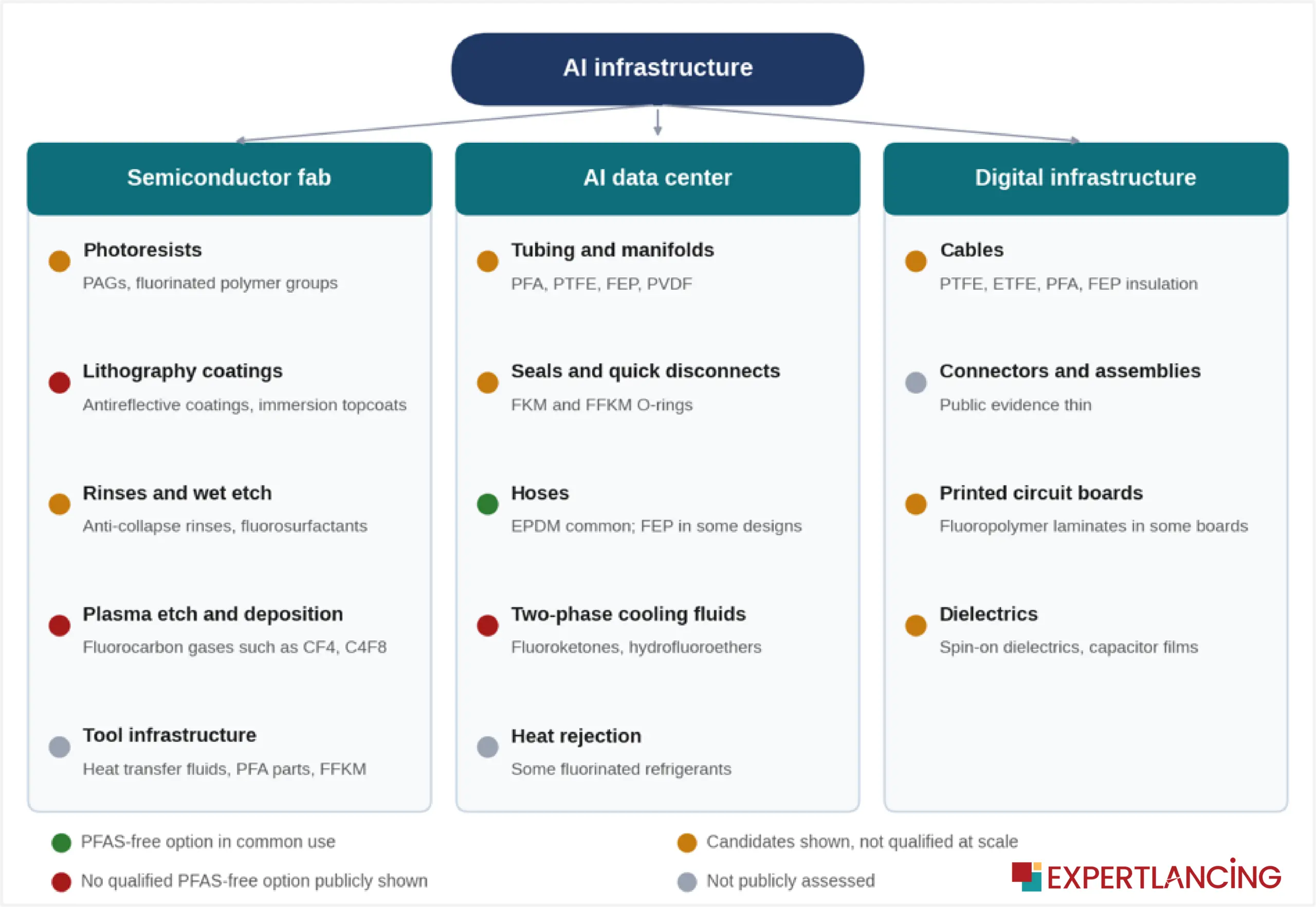
The EU defines PFAS by structure: any substance with at least one fully fluorinated methyl or methylene carbon, with narrow exclusions. By common estimates that covers more than 10,000 substances. A PTFE gasket, a photoacid generator and a two-phase coolant all qualify, yet share little beyond a carbon-fluorine bond. Each point in Figure 1 has its own function and difficulty of replacement, so a single “PFAS-free” target means little until it is broken down by application.
The Largest PFAS Volumes Are Not the Hardest to Replace
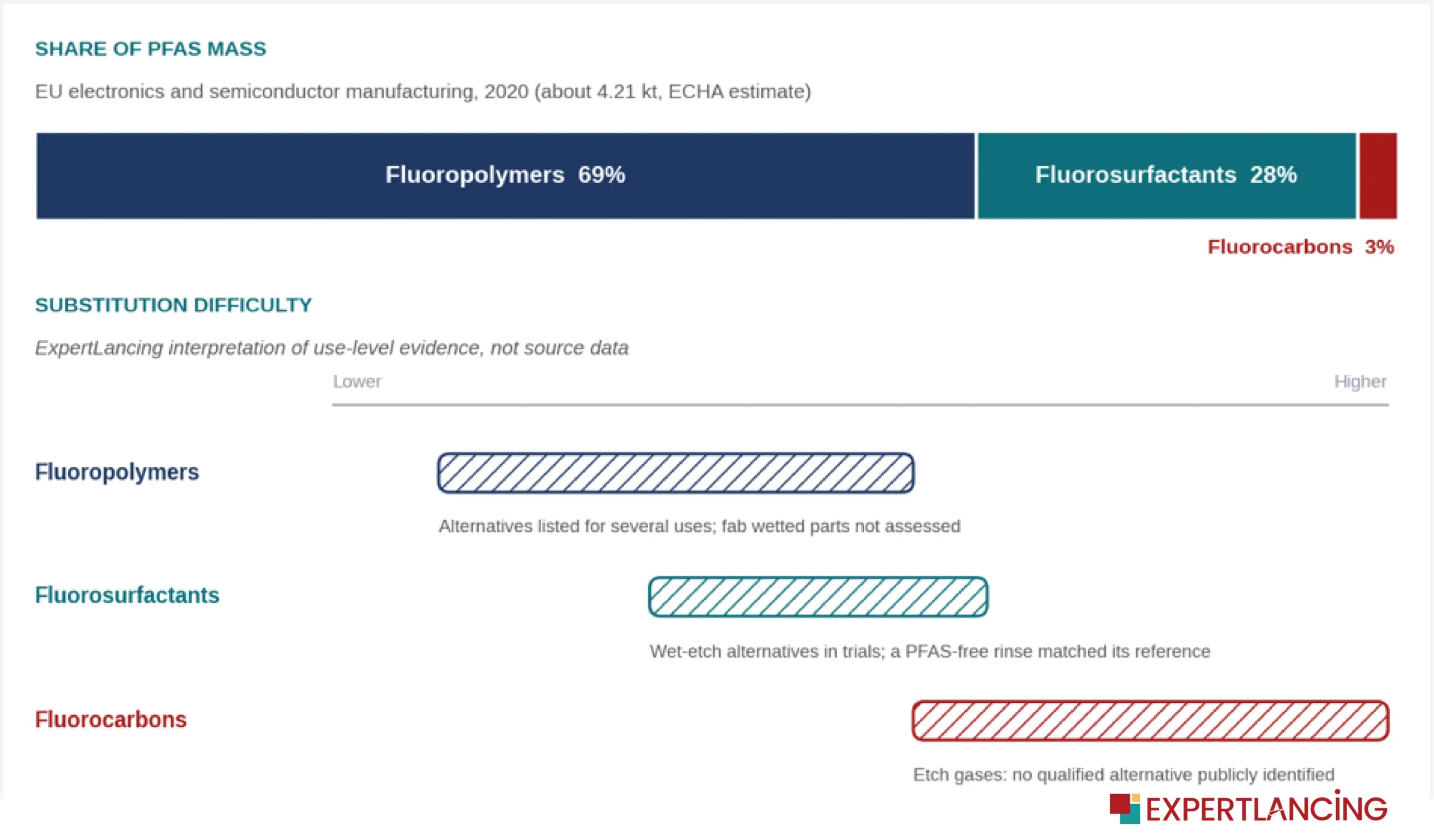
ECHA estimated that EU electronics and semiconductor manufacturing used about 4.21 kilotonnes of PFAS in 2020: roughly 69% fluoropolymers, 28% fluorosurfactants and 3% small-molecule fluorocarbons. The figure reaches most readers via a 2025 Harvard preprint citing a Nature feature; we could not trace it to ECHA’s own tables, so treat it as an order of magnitude.
For PFAS in semiconductor manufacturing, the split measures tonnage, not difficulty. The same preprint lists PFAS-free alternatives as available for several fluoropolymer uses, such as spin-on dielectrics, and none yet for the fluorocarbon gases used in dry etch.
These differences highlight why alternatives for PFAS in semiconductor manufacturing must be assessed application by application.
On our reading, the biggest category holds some of the most tractable cases and the smallest holds the hardest (Figure 2). Ranking the problem by tonnage would point effort in the wrong direction; the EU draft, sensibly, assesses exemptions use by use.
How AI Growth Affects PFAS Use in Semiconductor Manufacturing and Data Centers
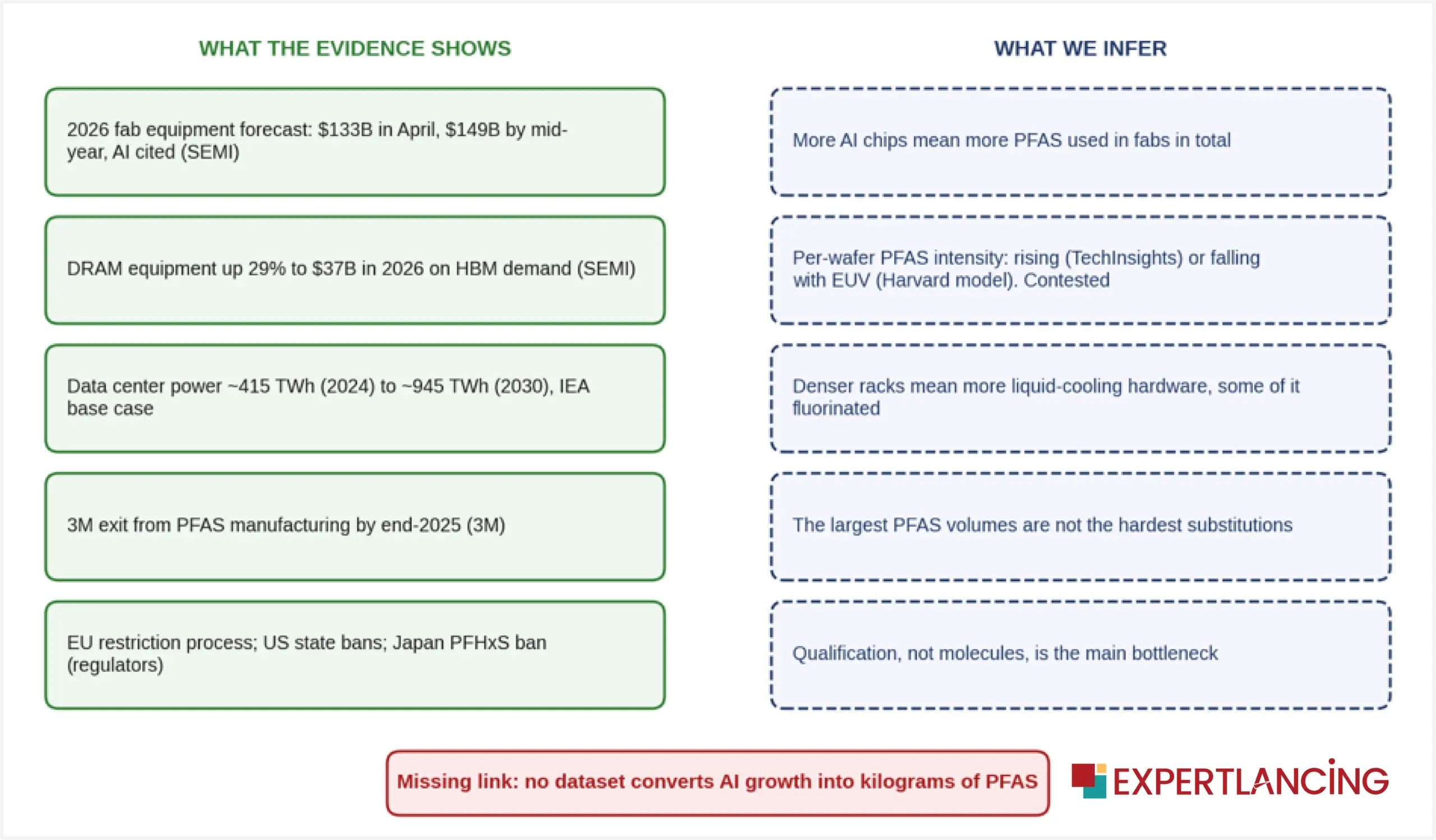
The IEA’s base case has data center electricity use rising from about 415 TWh in 2024 to about 945 TWh in 2030, with accelerated servers growing around 30% a year; its 2026 update keeps a similar path. But no public dataset converts AI capacity or fab capex into kilograms of PFAS, so any link is an inference, running through two channels (Figure 3).
The first is the fab. SEMI expects DRAM equipment spending to rise 29% to $37 billion in 2026 on AI-driven memory demand. More wafers mean more PFAS-containing steps in total; whether each wafer uses more is disputed. TechInsights argues that complexity at 4nm and 3nm offsets gains in individual steps; a Harvard model finds that at 7nm, extreme ultraviolet (EUV) patterning needed about 18% fewer PFAS-containing lithography layers than deep ultraviolet (DUV) multiple patterning.
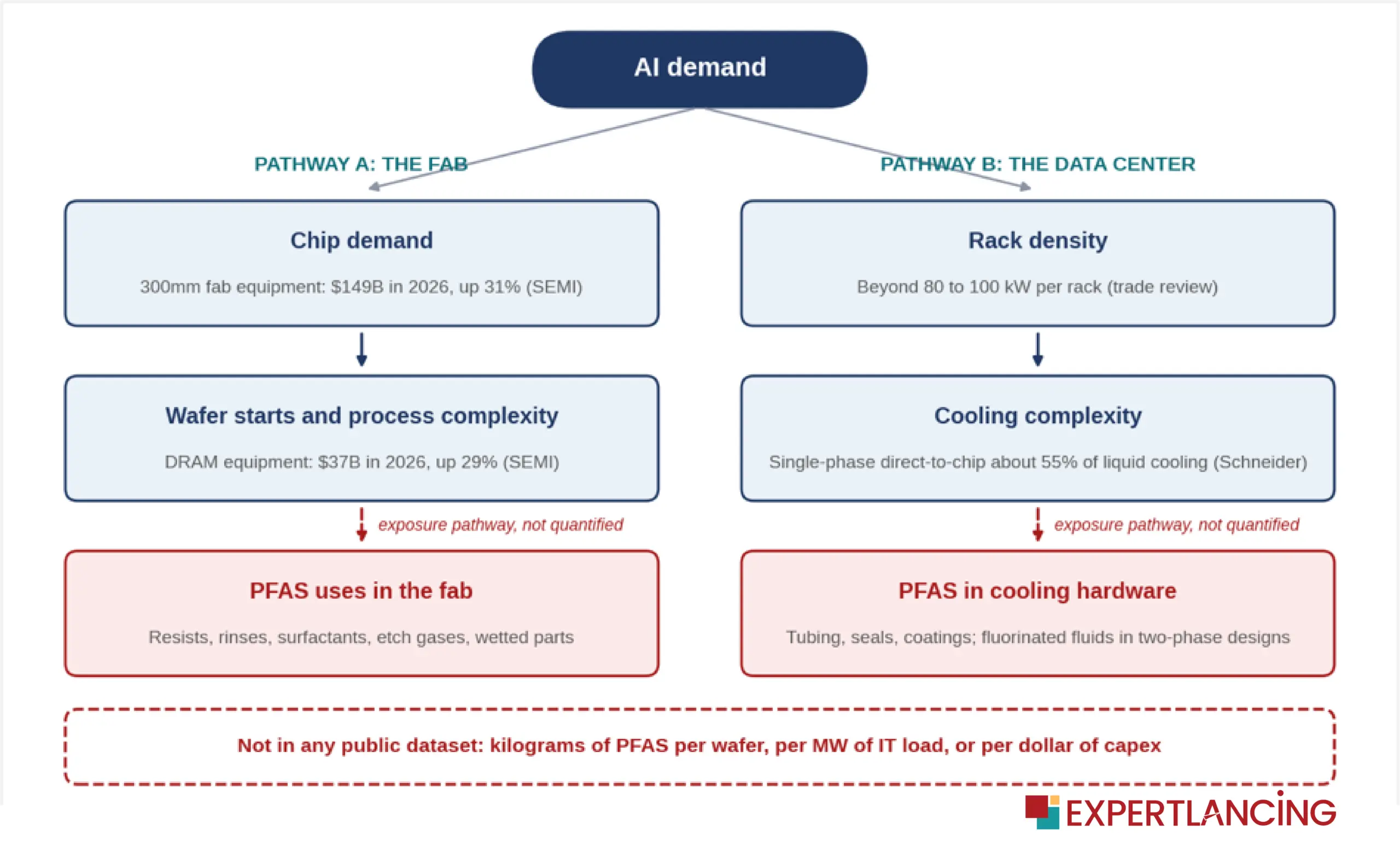
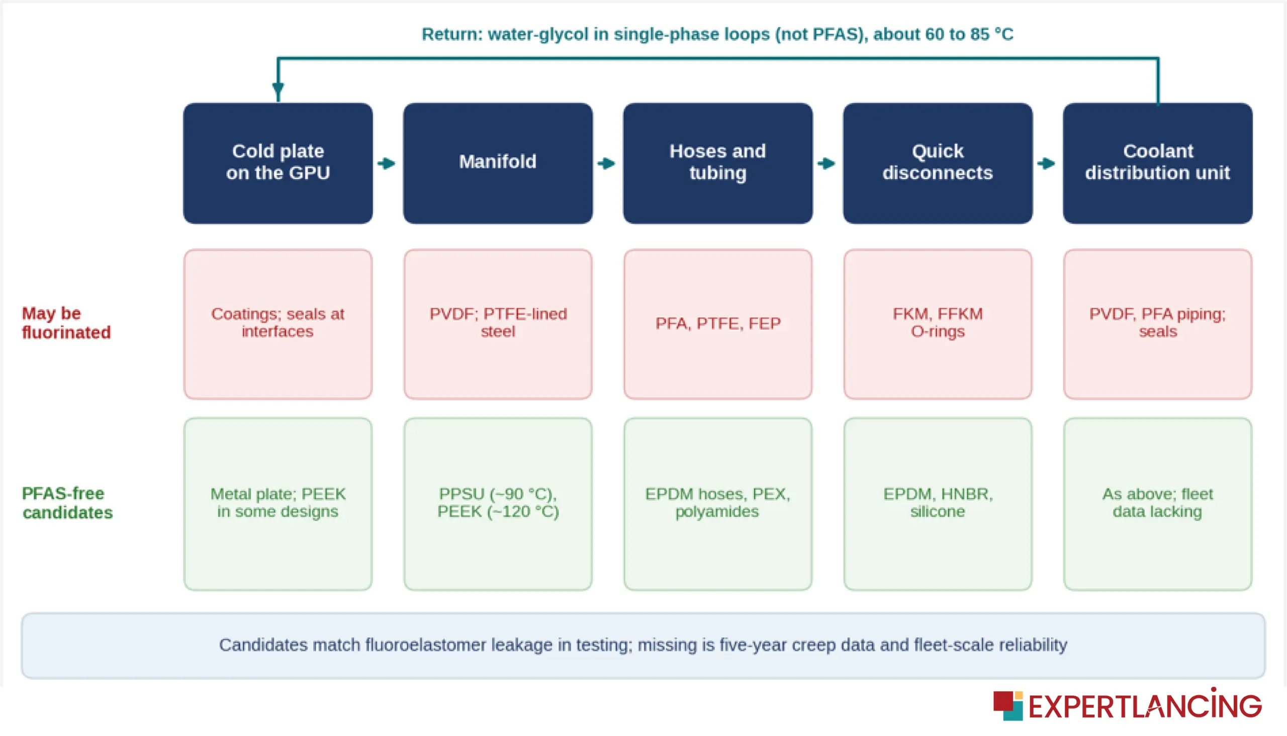
The second is the rack. A Plastics Engineering review reports AI rack densities beyond 80 to 100 kW, with direct liquid cooling now dominant in high-performance clusters, and Schneider Electric puts single-phase direct-to-chip cooling, which runs on water-glycol rather than PFAS, at about 55% of the market. Here the exposure sits in the hardware. The fab holds the hardest problems; the cooling loop holds most of the new hardware (Figure 4).
Cooling Hardware: Technical Feasibility Is Not Hyperscale Qualification
A direct-to-chip loop is a chain of wetted parts, from cold plate to coolant distribution unit, running at around 60 to 85 °C (Figure 5). The Plastics Engineering review says most systems use fluoropolymers such as PFA, PTFE, FEP and PVDF in tubing and manifolds, and fluoroelastomer O-rings in seals, though a tubing supplier says silicone and EPDM are the more common general-purpose seals. No independent data settles how much cooling hardware is fluorinated.
The PFAS-free candidates are credible. The review says EPDM, HNBR and silicone seals can match fluoroelastomer leakage with the right design. Engineering plastics such as PPSU and PEEK handle manifold temperatures. EPDM hoses are already common in water-glycol service and Meta reportedly evaluated EPDM hoses for Open Rack v3 in January 2026, according to a secondary source.
What is missing is time. The review lists five-year creep resistance as unresolved, and there is no public reliability data at fleet scale. A seal that passes a 1,000-hour laboratory test has not proven itself across thousands of racks, where one leak sits above a GPU.
In cooling hardware, the constraint is time in service, not chemistry.
Two-Phase Immersion: A Supplier Exit Moved Faster Than Any Rule
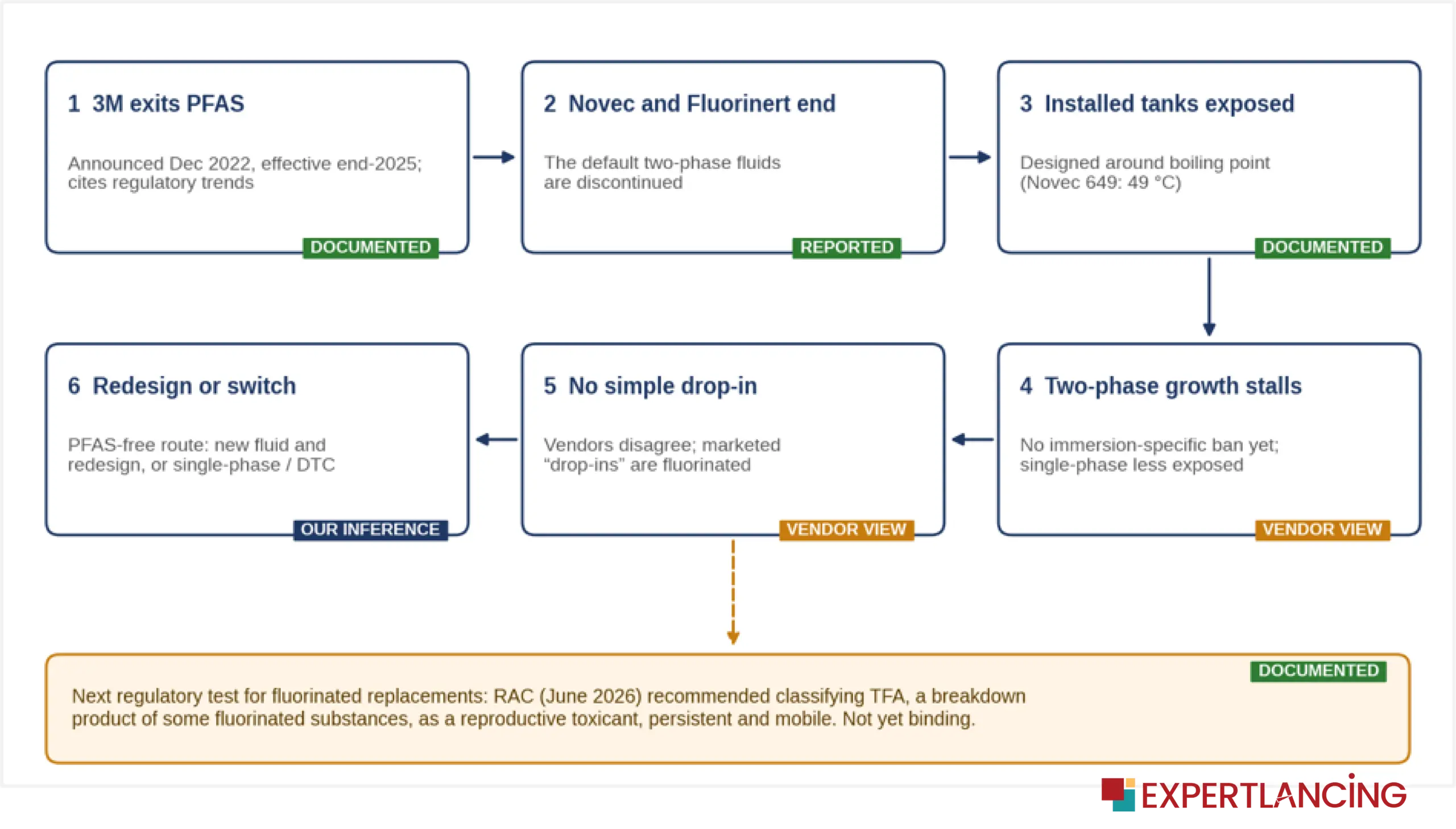
Two-phase immersion, where servers sit in a fluid that boils on hot components, is where the paradox has already moved a market, and the trigger was not a rule (Figure 6). In December 2022, 3M announced it would exit PFAS manufacturing by the end of 2025, citing accelerating regulatory trends. Its Novec and Fluorinert fluids, the default for two-phase tanks, went with it. Tanks are built around a fluid’s boiling point, 49 °C for Novec 649. Schneider Electric says no immersion-specific ban exists yet, but two-phase growth has stalled; single-phase systems are less exposed.
One distributor says no true drop-in exists; other suppliers sell “drop-in” fluids that are themselves fluorinated. Our reading: the closest drop-ins keep the tank design but not the PFAS exposure. And they face a second test. In June 2026, RAC recommended classifying trifluoroacetic acid (TFA), a persistent breakdown product of some fluorinated substances, as toxic to reproduction. The opinion is not yet binding.
Anticipated regulation reshaped this market before any binding restriction on immersion fluids existed.
Lithography: A PFAS-Free Resist Is Not Yet a PFAS-Free Fab
In the chemically amplified resists that dominate lithography, PFAS sits mainly in the photoacid generator (PAG), the ingredient that releases acid when light hits it and drives the patterning reaction. It also appears in antireflective coatings, immersion topcoats and rinses.
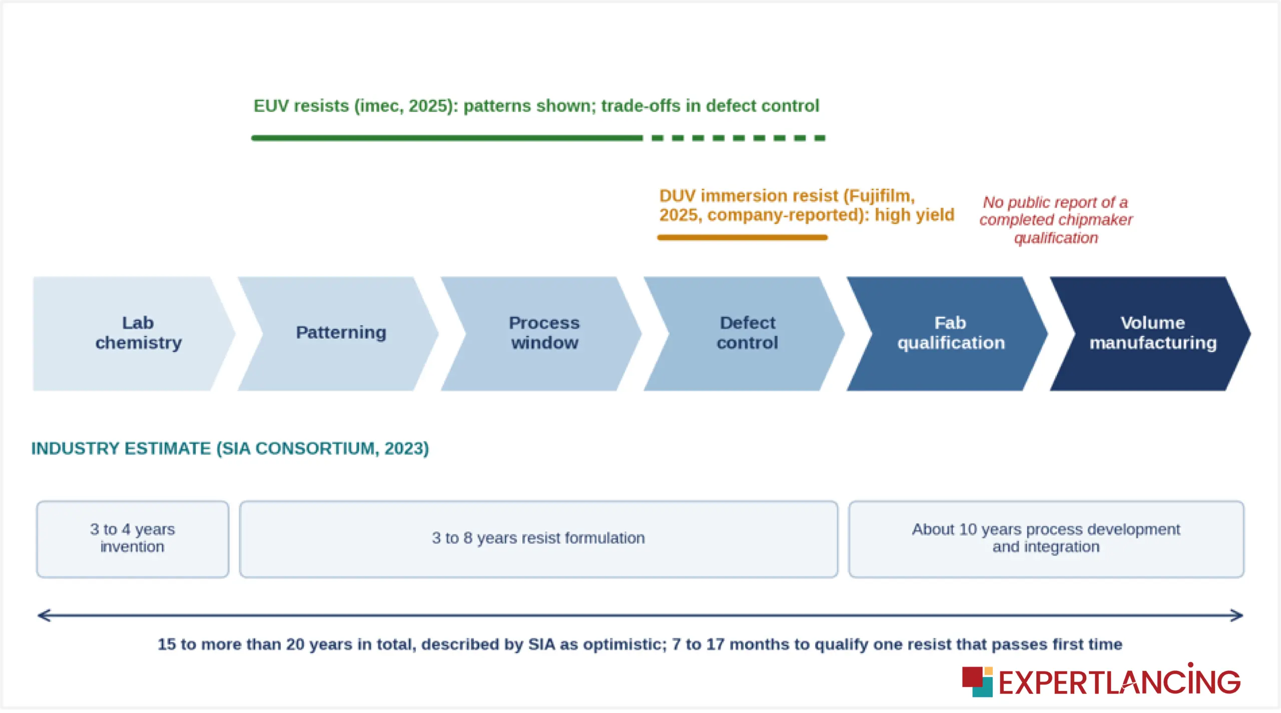
The technical news here is good. In initial tests reported in 2025, imec’s PFAS-free EUV resists patterned 32 nm pitch lines and 36 nm pitch contact holes about as well as PFAS-containing references. For DUV, Fujifilm announced a PFAS-free immersion resist that, evaluated with imec, achieved high yields in 28nm-generation metal wiring.
But imec also reported trade-offs in defect control and said antireflective coatings and immersion topcoats need entirely new approaches. The industry’s PFAS consortium, in a 2023 case study, put the optimistic timeline for replacing PAGs across all products at 15 to more than 20 years. That estimate comes from the party seeking exemptions and predates imec’s results, which suggest it is pessimistic for EUV, but nothing yet shows it is wrong for mature DUV layers. A resist that works in a controlled process is still years from volume manufacturing (Figure 7).
Plasma Etch: The Hardest Case Rests on the Thinnest Evidence
Plasma etch carves nanoscale features using fluorocarbon gases such as CF4, CHF3 and C4F8, which supply both the fluorine that etches and a thin fluorocarbon film that controls selectivity. Despite years of research, the Semiconductor Industry Association says researchers have not identified viable PFAS-free alternatives.
That is an industry claim resting partly on proprietary data. However, we found no public evidence of a qualified alternative, or independent assessment. Research on lower-emission gases such as C2F4O is active. Yet SIA’s own etch white paper notes that most PFAS definitions would capture such candidates. Much of this work swaps one fluorocarbon for another. And because SEAC found the proposed fluorinated-gas exemptions not justified as drafted, partly due to overlap with the EU’s F-gas Regulation, etch is unlikely to be settled by REACH alone.
PFAS Restrictions: Regulatory Timelines Across Major Markets
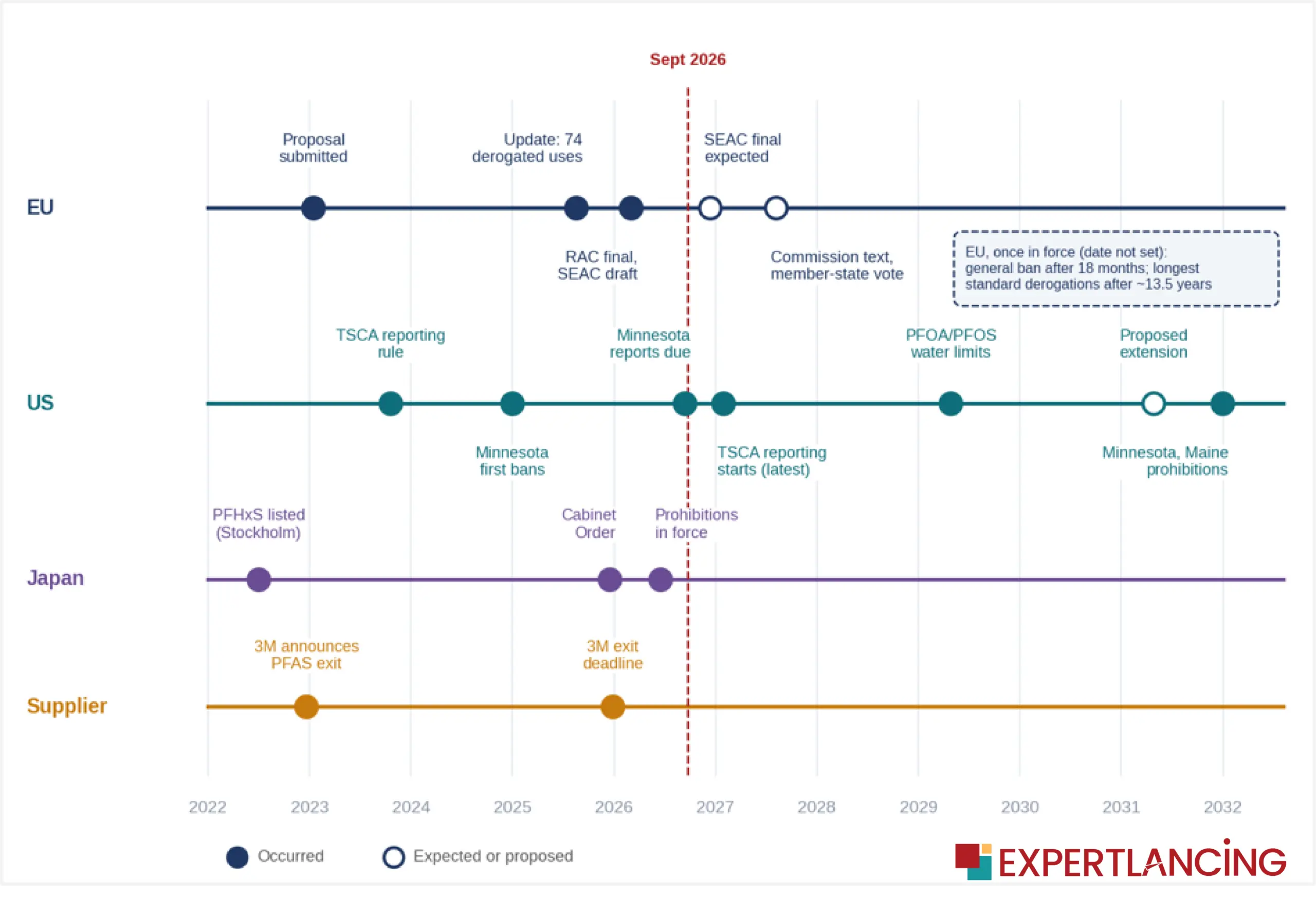
Regulation runs on at least three clocks (Figure 8). The EU is pursuing a class-wide restriction with use-specific, time-limited exemptions. An August 2025 update raised the number of exempted uses from 26 to 74, with phase-outs of up to 13.5 years after the rule takes effect. SEAC’s draft finds a full ban with a short transition unlikely to be proportionate, although the committees want many exemptions narrowed. Several electronics and semiconductor exemptions received a justified or likely justified assessment. One analyst reading, which we could not verify against the SEAC text, puts semiconductor manufacturing and circuit boards among the 12-year uses. Sealing, where cooling loops sit, was among eight late-added sectors the committees did not evaluate separately.
The United States is moving in two directions. The EPA has delayed PFAS reporting to no later than January 31, 2027, proposed exempting imported articles and proposed more time for water utilities to meet PFOA and PFOS limits. The states are tightening: from 2032, Minnesota prohibits products with intentionally added PFAS unless a use is ruled “currently unavoidable”, including internal electronic components, and Maine has a similar rule. For a multinational, the binding regulator is often a US state or Brussels, not Washington.
Japan is narrower and already in force. Since June 17, 2026 it has prohibited in principle PFHxS-related substances, a group listed under the Stockholm Convention, and banned imports of listed products containing them, including semiconductor etching agents and photoresists.
There Is No Single PFAS Substitution Problem
Put the cases side by side and they separate (Figure 9). Cooling seals and hoses are furthest along. EUV resists show strong technical progress with little public qualification data. DUV resists and interconnect dielectrics sit lower: the first because of the installed base, the second because, beyond supplier descriptions of fluoropolymer cables, we found no independent assessment of PFAS-free options for high-speed interconnects. Plasma etch and like-for-like two-phase fluids sit at the bottom, though immersion has an exit, a change of architecture, that etch lacks.
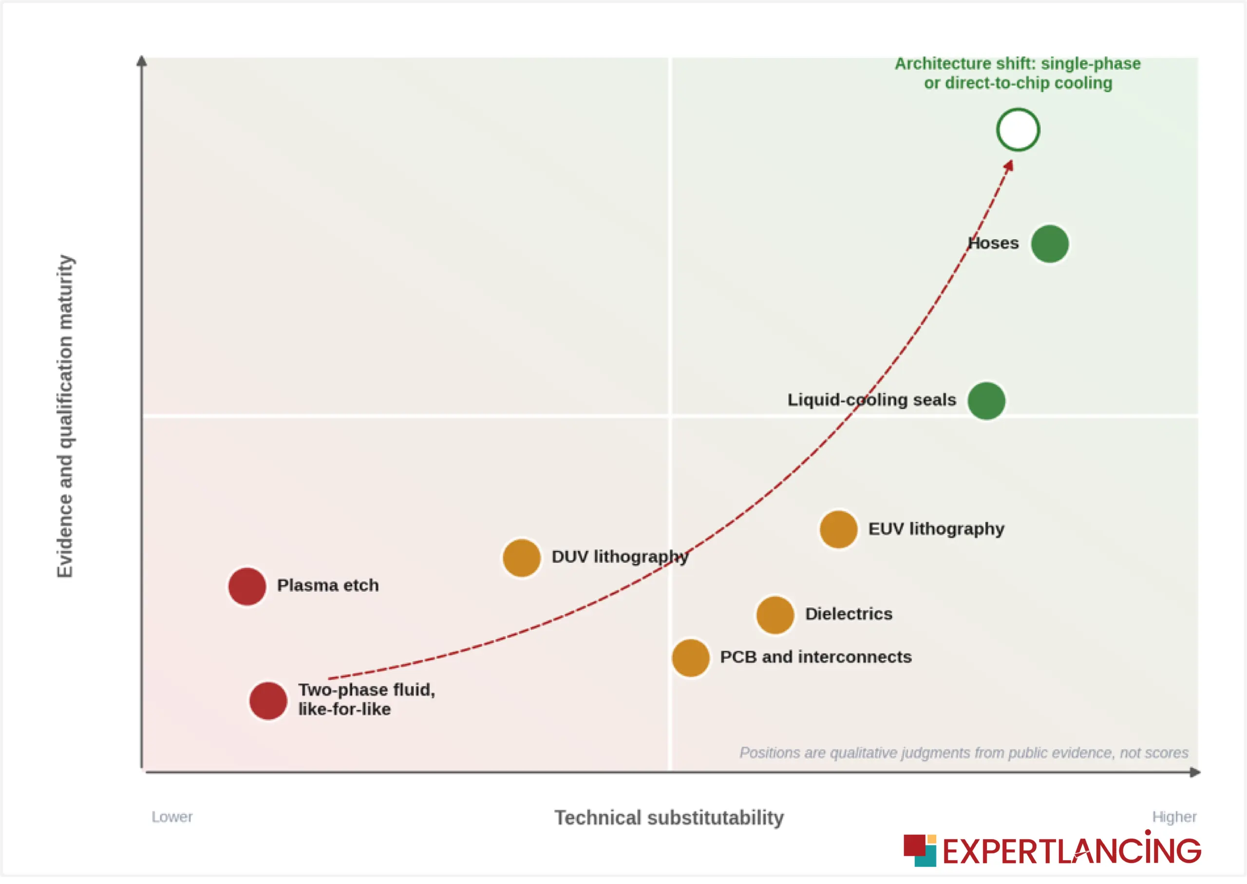
Every substitute must also clear four barriers.
- Performance: does it deliver the function? Etch gases and PAGs fall short today.
- Reliability: does it last for years in real conditions? That is the open question for cooling seals.
- Qualification: can it pass fab or data center qualification in time? Even one resist that passes first time takes 7 to 17 months, on SIA’s estimate.
- Regulatory durability: will it face the next round of rules? This is the barrier most often skipped. Fluorinated immersion fluids face the TFA question, and lower-emission etch gases still count as PFAS. Swapping one fluorinated molecule for another can clear three barriers and fail the fourth.
The Critical Gap Is Between Transition Periods and Qualification Timelines
The clocks start at different points, so compare them with care. The longest standard EU exemptions end about 13.5 years after a start date not yet set. The industry’s 15-to-20-year PAG estimate runs from the start of research, and imec’s PFAS-free program began in 2023. The gap’s size is uncertain, but its shape is clear. It is small in cooling hardware, where the constraint is reliability data. In two-phase immersion, a supplier exit got there first. It is widest in the fab, in DUV lithography additives and etch gases.
WHAT TO WATCH
- SEAC’s final opinion (expected by end-2026) and the Commission’s legal text
- The EPA’s final PFAS reporting rule, due before the January 31, 2027 backstop
- Commission action on the TFA classification
- Minnesota and Maine decisions on “currently unavoidable” uses
- Qualification data for PFAS-free resists beyond EUV, and for non-fluorinated two-phase fluids
A Qualification Race, Not a Chemistry Swap
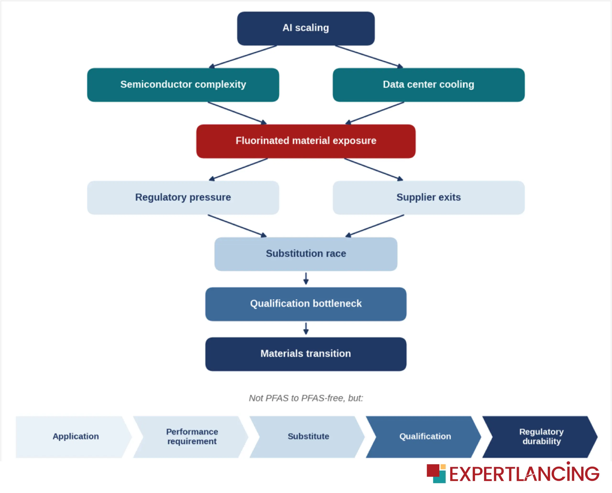
The transition is not simply PFAS to PFAS-free. It runs from application, to performance requirement, to substitute, to qualification, to regulatory durability; the molecule is only the third step (Figure 10). That makes it a materials qualification race. Where candidates exist, the pace is set by time-in-service and yield data, which is hard to compress. Where they do not, as in etch, the clock has not started. And every substitute must survive the next regulatory round.
For operators, the practical step is to map exposure at component level and start qualifying substitutes wherever they exist. Reliability data takes years to build. For suppliers and investors, the advantage is likely to go to qualified, regulation-durable PFAS-free positions rather than to candidate molecules. On current evidence, the most exposed look like fluorinated two-phase fluids and legacy lithography chemistry. That is our reading, not a forecast.
In this transition, the first qualified alternative is likely to matter more than the first alternative.
The PFAS Transition: From Regulatory Risk to Strategic Decisions
The PFAS paradox will not be resolved by a single ruling or a single molecule. It will be resolved application by application, on whichever clock reaches its deadline first: a regulatory phase-out, a qualification cycle, or a supplier’s decision to exit a chemistry altogether, as 3M already has. Cooling hardware can move now, constrained mainly by time in service. Lithography has working prototypes still years from volume production. Etch chemistry has no credible substitute at all, and its clock has not yet started. What connects these cases is that the molecule is rarely the hard part; qualification, reliability and regulatory durability are. For companies across this value chain, the practical task is not to wait for certainty but to map their own exposure now, qualify what can be qualified, and treat every fluorinated substitute as provisional until it too survives the next round of rules.
Expertlancing helps organisations navigate such technology transitions through IP research, technology advisory, and market intelligence. Its capabilities span patent landscape analysis, technology scouting, competitive intelligence, and market research. By combining patent data with technical and market insights, Expertlancing helps clients track emerging technologies. It also helps assess alternative materials, monitor competitor developments, and identify potential risks and opportunities across evolving technology landscapes.
With a team of 60+ professionals in India and a global presence across the USA and Japan, Expertlancing brings together IP researchers, technical experts, and domain specialists. Together, they examine innovation and technology shifts from multiple perspectives.
Looking to assess emerging material alternatives, track technology developments, or understand the competitive implications of evolving PFAS regulations? Connect with our experts to discuss your research needs and explore how our IP intelligence and technology advisory capabilities can support your next strategic decision.