
The semiconductor industry is shifting in ways we haven’t seen in two decades. Here’s the reality for India: more than 90% of the chips this country needs come from abroad. When pandemic, we all learned how risky that is. Now, with the US-China tension, every major company is looking for Plan B. India is suddenly on the shortlist.
Why? Three things: deep engineering talent, a stable democracy, and an electronics manufacturing base that keeps growing. The India Semiconductor Mission launched with ₹76,000 crore, and that changed the game. By August 2025, they had approved ten projects across six states totaling some ₹1.6 lakh crore.
But here is the practical question every founder, investor, and executive I talk to keeps asking: Do I build a fab, or do I go fabless? This article breaks down both paths with real numbers and honest assessments of what works and what doesn’t.
Understanding the Two Business Models: Capital Intensity vs. Design Agility
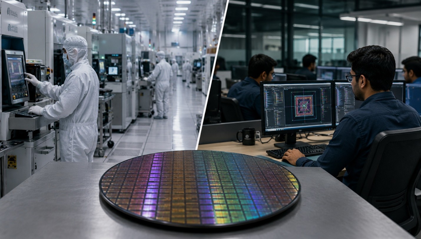
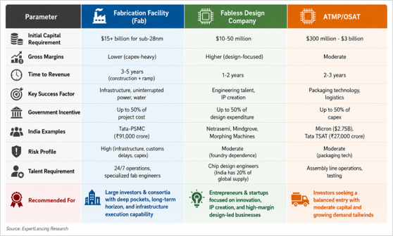
India’s chip ambitions rest on a handful of business models that look nothing alike, they differ in how much capital they lock up, how much risk they shoulder, and what margins they leave behind. At the heaviest end sit the fabrication plants, or fabs. Standing up a sub-28nm foundry can run past $15 billion for a single site, because the work hinges on costly extreme ultraviolet (EUV) lithography tools, rooms kept obsessively clean, and production lines that never pause, day or night. What rolls out of these plants are the silicon wafers that underpin every electronic device in existence.
Fabless companies take the opposite tack. Their energy goes into design, chip architecture, and the intellectual property behind it, while the manufacturing itself is handed off to outside foundries, most of them clustered in Taiwan, South Korea, and China. Since their outlay rarely stretches beyond design software, skilled engineers, and routine working capital, the model demands far less cash, and it tends to generate gross margins that outpace those of the foundries doing the fabrication. The catch is control. By depending on someone else’s factories, a fabless firm surrenders its say over production timelines and yields; in return, it gains flexibility and a faster path to market.
A third route is steadily catching on in India: Assembly, Testing, Marking, and Packaging (ATMP), also known as Outsourced Semiconductor Assembly and Test (OSAT). These operations sit between the two extremes, offering respectable profitability without the punishing capital bill that full-scale fabrication carries. The country’s first facility of this kind – Micron Technology’s $2.75 billion plant in Sanand, Gujarat, is proof that the middle path can hold up in practice.
India’s Evolving Semiconductor Ecosystem: From Design Services to Manufacturing
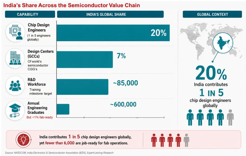
For most of its history, India’s place in the semiconductor world sat firmly on one side of the business: design. Over several decades it grew into a major center for design services, and even today close to a fifth of the world’s chip design engineers work out of the country. That talent kept the research and development arms of firms like Intel, Qualcomm, and Broadcom running, and yet, for all that design muscle, almost nothing was actually being manufactured on Indian soil. Closing that gap, and pushing the country further up the value chain from design into production, is precisely what the ISM was built to do.
The approved projects under the Mission reflect a carefully calibrated portfolio approach. At the high end, Tata Electronics has partnered with Taiwan’s Powerchip Semiconductor Manufacturing Corporation (PSMC) to establish India’s first indigenous semiconductor fab in Dholera, Gujarat. This ₹91,000 crore investment will manufacture power management ICs, display drivers, microcontrollers, and high-performance computing logic, with a planned capacity of 50,000 wafers per month. Complementing this are OSAT facilities in Assam, Uttar Pradesh, and Gujarat, creating a distributed manufacturing footprint that reduces geographic concentration risks.
The fabless ecosystem, meanwhile, has demonstrated significant growth and innovation. 2025 saw steady progress in the semiconductor startup landscape, highlighted by notable Series A fundraises for companies like Netrasemi, Mindgrove, and Morphing Machines. The government’s Design Linked Incentive (DLI) Scheme, which reimburses up to 50 percent of eligible design expenditure, has catalyzed entrepreneurship in areas ranging from edge AI and IoT to automotive semiconductors and RISC-V cores.
Strategic Considerations: Choosing Between Fab and Fabless
The decision between pursuing a fab or fabless model hinges on several critical factors that prospective entrepreneurs and investors must carefully evaluate. Market opportunity represents the primary consideration. While India’s semiconductor demand continues to grow across sectors, significant differences exist across market segments. Mature nodes (28nm and above) serve automotive, industrial, and power applications where India has growing domestic demand, while advanced nodes (below 7nm) cater to high-performance computing and AI workloads where global supply chains remain concentrated.
Access to capital and the willingness of investors to commit resources represent another critical consideration. Fabless ventures can achieve meaningful scale with funding in the range of $10-50 million, making them accessible to venture capital investors. In contrast, fab projects require billions of dollars in equity and debt financing, typically necessitating sovereign wealth funds, strategic corporate investors, or government participation. The Tata-PSMC partnership exemplifies this reality, with the Government of India providing fiscal support of up to 50 percent of project cost under the Semiconductor Fab scheme.
Infrastructure readiness presents particular challenges for fab projects. Semiconductor manufacturing requires uninterrupted electricity supply, high-purity water, and advanced waste management systems. While the Dholera Special Investment Region offers dedicated infrastructure, other locations face constraints. Customs regulations add weeks and months of delay into shipments of critical equipment, and existing labor codes do not optimally accommodate the 24-hour cycle times required for continuous fab operations. Fabless companies face fewer infrastructure constraints, though they remain dependent on foreign foundries for manufacturing.
Trends That Are Changing the Market
Several trends are reshaping the semiconductor business in India.
Open Architecture and RISC-V
The rise of domain-specific architectures and the RISC-V open instruction set architecture is lowering barriers to entry for fabless companies. Unlike proprietary architectures that require expensive licensing fees, RISC-V allows Indian startups to develop competitive processors without heavy upfront IP costs. Companies like InCore Semiconductors and Mindgrove Technologies are using this trend to build indigenous processor designs.
Compound Semiconductors
The compound semiconductor market, including silicon carbide (SiC) and gallium nitride (GaN) devices for power electronics, is emerging as a strategic priority. These materials are essential for electric vehicles, renewable energy systems, and high-efficiency power supplies. The approval of SiCSem’s project in Bhubaneswar marks India’s entry into this specialized segment. This offers more manageable capital requirements than silicon CMOS fabs while serving high-growth applications.
Geopolitical Realignment
Geopolitical changes are creating new partnership opportunities. The United States has established a partnership with the India Semiconductor Mission to explore supply chain diversification. Japan and India have agreed to collaborate on semiconductor development. These multilateral engagements help with technology transfer, workforce development, and market access. This benefits both fab and fabless ventures.
Future Outlook: The Convergence of Design and Manufacturing
Looking ahead, the distinction between fab and fabless approaches may gradually reduce as India’s ecosystem matures. The most successful semiconductor businesses will likely use hybrid strategies. They will keep fabless operations for rapid innovation while securing capacity commitments or partnerships with domestic fabs for critical products. This model, already common among established global players, allows companies to optimize the trade-offs between capital efficiency and supply chain security.
The Tata fab, when operational, will change the competitive landscape significantly. By providing indigenous manufacturing capacity for mature nodes, it will allow fabless companies to serve customers with domestic content requirements or supply chain security concerns. This relationship between fabs and fabless companies will be essential for building a self-sustaining ecosystem.
However, significant challenges remain. Import dependence for critical inputs, including silicon wafers, specialty chemicals, and advanced equipment, continues to limit the industry. Addressing these bottlenecks will require targeted investments in materials science, precision manufacturing, and logistics infrastructure. The Semiconductor Mission 2.0, announced in early 2026, aims to address these gaps by focusing on producing semiconductor equipment and materials in India.
Related Opportunity: AI Hardware and Edge Computing
As semiconductor businesses think about their positioning, the intersection of artificial intelligence and hardware presents interesting opportunities. The growth of AI workloads at the edge, from industrial automation to autonomous vehicles, is driving demand for specialized AI accelerators and neural processing units. Indian fabless companies are well-positioned to address this segment by developing chips optimized for specific use cases and price points. For businesses considering entry into the semiconductor sector, exploring the AI hardware ecosystem and its connection with India’s growing electronics manufacturing capabilities could reveal additional ways to create value. This area represents a natural extension of the fabless model, using India’s software and algorithmic strengths in AI alongside hardware design capabilities.
Conclusion: A Dual-Track Strategy for India Semiconductor Success
The choice between fab and fabless is not a simple either-or decision. It depends on your specific situation. For entrepreneurs and investors with deep technical expertise, patient capital, and the ability to navigate complex regulations and infrastructure requirements, the fab path offers the potential for substantial market share in the rapidly growing domestic market. For those who want capital efficiency, speed to market, and flexibility, the fabless model aligns with India’s established strengths in design and engineering talent.
The best approach for India’s semiconductor ecosystem is a dual-track strategy: supporting the development of indigenous manufacturing capabilities while simultaneously building a strong fabless design ecosystem. The government’s incentive schemes recognize this by providing fiscal support across the value chain, from design-linked incentives to fab construction subsidies.
Whether through pioneering fabs or innovative fabless designs, the opportunity to build world-class semiconductor businesses in India has never been better. The question is not whether India will play a significant role in the global semiconductor industry, but rather which path, or combination of paths, will allow individual businesses to capture the most value from this historic transformation.